By Chris Vineis, Moran Levy-Finklshtein, James Carey, Greg Knight, Eckard Wefringhaus, Rudolf Harney
.jpg)
.jpg)
Standard Chemical Surface Texturing
Although crystalline silicon represents the overwhelming market share of solar cells, it is not a very efficient light absorber due to its indirect bandgap. Silicon cells are therefore still relatively thick, typically 180-200 m, and require high-quality surface texture to reduce surface reflectance and improve light trapping. The ideal surface texture would exhibit many properties simultaneously, including very low reflectance at all incidence angles, good light trapping that increases the optical path length inside the solar cell, and physically robust features that are easy to passivate and metalize.
For monocrystalline silicon, with a (100) surface orientation, the solution that is commonly used in industry is anisotropic etching using KOH and IPA. The alkaline chemical preferentially etches (100) planes and stop on (111) planes, thus creating surface pyramids. These pyramids are typically 5-10 m in height and randomly located across the surface. Surface reflectance is reduced since incoming light rays experience multiple bounces off the pyramid faces, allowing light more chances to propagate into the solar cell. On average, each beam bounces a little more than twice, reducing the minimum reflectance to ~10% (before anti-reflective coating) at ~900 nm, in comparison to a value of ~35% for a bare polished silicon wafer. This technique is very robust and reproducible, and after anti-reflective coating yields a very low surface reflectance. A few downsides to this process are that it is slow (standard process is 25-35 minutes, although some novel processes under development are ~10 minutes) and thus not amenable to inline processing, and since the pyramid facets are smooth the surface reflectance is very dependent on incidence angle. The latter issue can affect light collection efficiency depending on time of day.
For multicrystalline silicon, which is the dominant technology for solar cells today, anisotropic etches are not suitable due to the variety of crystal grain orientations present on the surface. The industry-standard solution today is an isotropic etch comprising HF and HNO3 acid, commonly referred to as isotexture. This etch forms texture by preferentially attacking areas of crystalline damage, which are present from residual saw damage in the wafer. The process simultaneously removes some saw damage and forms a scalloped surface texture, and is fast enough to be performed with an inline tool. However, it has numerous drawbacks, most importantly that it is not able to simultaneously maximize both cell voltage and current. One reason for this is that rougher isotextured surfaces that lower reflectance have large surface area and can be difficult to passivate, while smoother surfaces that are easily passivated have poor (high) reflectance. Another reason is that the isotexture process typically still leaves residual saw damage in the wafer, since deeper etching that would completely remove the saw damage would also result in a fairly non-textured surface. Additional drawbacks of the isotexture process are that it is fairly dependent on the exact HF:HNO3 ratio, and it has a high process variation because of different behavior exhibited by the various crystal grains.
Ultrafast Laser Surface Texturing
SiOnyx has developed a patented1) ultrafast laser process to texture the surface of a silicon wafer, which offers several advantages over chemical texturing including low reflectance, independence of crystal grain orientation, single-sided touch-less process, suitability for inline processing, and a very low profile topography that is physically robust. For multicrystalline wafers, it has the added benefits of breaking the (isotexture) tradeoff between cell current and voltage, and reducing process variation.
The pioneering work into the use of ultrafast laser processing of semiconductors was carried out at Harvard University in the lab of Prof. Eric Mazur starting more than a decade ago.2),3) Fundamental experimentation at Harvard laid the foundation for understanding the interaction of short pulse lasers with silicon and how to engineer the properties of the lased material. SiOnyx was spun out of Harvard in 2006 with the goal of commercializing this technology, and we have since made numerous modifications to adapt the technology for industrial applications.
The SiOnyx laser texturing process is performed in open air, and a throughput of over 1,200 wafers per hour is viable with just a single ultrafast laser at today’s commercially available laser powers. Depending on the lasing conditions, a wide range of surface textures and visual appearances are achievable, as shown in Figure 1. This is an image of a multicrystalline Si wafer that has been lased using various fluences and pulse densities. Incredibly dark surfaces with reflectance below 5% can be achieved, which is why the process is often referred to as ‘Black Silicon’. Importantly, the laser texturing process is independent of crystal grain orientation, as can be observed for most texture squares where the crystal grains are no longer observable. This improvement in visual uniformity manifests itself as a tighter binning of cell efficiencies compared to standard isotexture, as discussed in the cell processing results section.
.jpg)
Typical surface texture for SiOnyx’s process is shown in an oblique-angle scanning electron microscope image in Figure 2. The peak-to-valley height of the undulating features is less than one micron, and the entire texturing process consumes less than two microns of silicon. As a result the surface is easily passivated and metalized using standard solar tools and processes. This is an important improvement over earlier ‘Black Silicon’ texturing processes that created very large (>5 m) conical-shaped features that can be difficult to process and may not be physically robust. Thus, the SiOnyx laser texturing technique is highly amenable to today’s silicon solar cells, ultra-thin silicon wafers anticipated in the future roadmap, and non-silicon thin-film solar technologies today that are material-thickness constrained.
Reflectance curves comparing various textures (before addition of anti-reflection coating) are shown in Figure 3. A major downside to isotexture as noted before is that the reflectance is not very low, as shown by the dashed red curve. SiOnyx’s laser texture on multicrystalline silicon (solid black curve) achieves a significantly lower reflectance, almost as low as alkaline etching on monocrystalline silicon (dash-dot green curve). The laser texture results in a solid efficiency boost over isotexture and tighter efficiency binning--with no changes required to downstream cell processing tools--as discussed in detail in the next section. Finally, the dotted black curve shows the demonstrated potential for SiOnyx’s laser texturing on multi- or monocrystalline silicon. This very low and spectrally-flat reflectance represents a significant improvement over both acidic isotexture and alkaline etching and could enable large efficiency boosts: over 1% (absolute) is anticipated for multi-Si with an optimized process flow.
.jpg)
.jpg)
Ultrafast Laser-Textured Multicrystalline Solar Cells
In order to demonstrate the benefit of SiOnyx’s laser texturing for multicrystalline silicon solar cells, SiOnyx collaborated with German research institute ISC Konstanz for cell processing and testing. Standard 156 mm multicrystalline wafers were processed using screen-printed metal, aluminum back surface field, front-side silicon nitride anti-reflective coating and passivation, and a standard diffused emitter. A comparison was made between cells receiving standard isotexture, isotexture etch combined with SiOnyx’s laser texture, and deep acid polish etch followed by SiOnyx’s laser texture. The first two groups of wafers were ~170-180 m thick, while the third group was much thinner (~150-160 m) due to the deep acid polish etch removing ~8-10 m of silicon per side. Typical reflectance curves for the laser texture were shown as the solid black line in Figure 3. Laser texturing was performed using a Coherent AethonTM tool with a TaliskerTM picosecond laser.
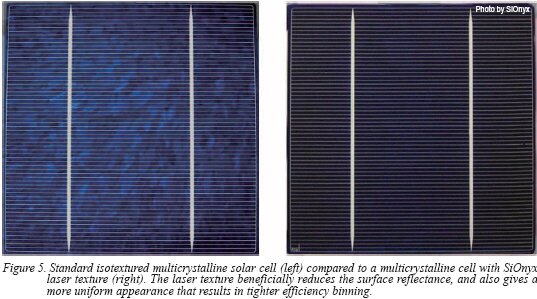
An efficiency improvement of 0.3% (absolute) was measured for the cells that received laser texture on top of isotexture, compared to isotexture only, as shown in the histogram plot in Figure 4. The average efficiency for the laser-textured cells was just over 17%. An important point is that not only is the efficiency increased, but in addition the process variation is reduced. Efficiency binning is improved by a factor of 2x for laser texture compared to isotexture, a benefit we have observed on numerous cell lines. This improvement is due to tighter cell current distributions enabled by the more uniform surface achieved using laser texture compared to isotexture, as seen in Figure 5. As a result, the problematic low-end tail of the distribution can be reduced or eliminated, which goes directly to the cell manufacturer’s revenue and profit margin.
The 0.3% (abs.) efficiency improvement was achieved due to an increase in short-circuit current density (Jsc), with no degradation in open-circuit voltage (Voc) or Fill Factor (FF). Specifically, average Jsc values of 34.4 mA/cm2 were achieved for the laser-textured cells, compared to 33.8 mA/cm2 for isotexture-only cells. Voc ranged from 625 to 630 mV for both sets of cells, while FF values ranged from 78.5 to 79.5% for both sets of cells. The fact that Voc and FF were not degraded for the laser-textured cells confirms that there is no residual damage from the SiOnyx process. This is because the so-called ‘heat affected zone’ from ultrafast laser processing can be 0.2 m or even less, thus requiring little post-laser processing, in contrast to nanosecond laser texturing where the thickness of the damaged layer can extend upwards of 20 m into the substrate.4) The good Voc and FF values also confirm that the SiOnyx laser texture is easily passivated and metalized. These are all critical points to ensure easy technology adoption. No modifications to the downstream cell processing steps such as POCl3 diffusion, nitride deposition, screen printing or firing are required in order to take advantage of this superior surface texture.
The third group of multicrystalline Si cells processed and tested at ISC Konstanz received a deep acid polish etch followed by single-sided laser texture. Despite the fact that these wafers were fairly thin (150-160 m), they maintained excellent efficiency values with an average of 16.9%. This represented a nearly 0.2% (abs.) efficiency boost over the thicker isotextured baselines, and was achieved because of slightly higher Voc values (a benefit of this process compared to isotexture) as well as good Jsc values due to the excellent light trapping properties of the SiOnyx laser texture. Continuous migration to thinner wafers is a key part of the solar roadmap due to the direct cost savings, since silicon raw material is still the dominant cost in a module. In addition, this specific process flow is ideal for roadmap architectures using backside dielectric passivation with local metal contacts, since the backside is planar while the front is textured.
A final important point is that the efficiency boost obtained using laser texturing occurs due to enhanced Quantum Efficiency (QE) in the red and near-infrared portion of the solar spectrum. Thus, SiOnyx’s technology is complementary to other efficiency boosts such as selective emitter (which boosts blue QE), advanced metal pastes, and backside passivation that are in production or on the roadmap today.
SiOnyx’s proprietary ultrafast laser texturing offers many benefits compared to standard wet chemical texturing techniques, and is now an economically attractive process for the solar industry due to continued improvements in laser power5) and reduction in laser costs. A 0.3% absolute efficiency boost was demonstrated using laser texture on multicrystalline silicon compared to standard isotexture, with the laser-textured cells averaging just over 17% efficiency. In addition, the SiOnyx laser texturing process results in tighter efficiency binning compared to isotexture, and maintains high efficiencies even for thinner silicon cells. Importantly, the combination of efficiency boost, tighter efficiency binning and thinner wafers results in a lowered US$/Wp cost for the cell manufacturer. SiOnyx’s process can be seamlessly integrated into existing cell lines to give an immediate boost to both efficiency and the bottom line, and is highly compatible with nearly all future roadmap solar cell architectures.
Dr. Christopher Vineis is the Director of Solar Technology at SiOnyx (www.sionyx.com). He has over 15 years of experience in semiconductor material processing and device development. Dr. Vineis’ Ph.D. is from Massachusetts Institute of Technology in materials science and engineering.
Moran Levy-Finklshtein is a Process Engineer at SiOnyx focused on solar cell development, and has over 7 years of experience in process development, optimization and sustaining. She received her Bachelor’s and Master’s degrees in Material Science from Ben-Gurion University.
Dr. James Carey is the Director of laser process development at SiOnyx. He graduated from Harvard with his Ph.D. in Applied Physics and has a B.S.E. in Engineering Physics from the University of Michigan.
Greg Knight is a consultant at SiOnyx. He has over 10 years of process, manufacturing and R&D experience in crystalline photovoltaics. Currently he is President of PV Tech Group, LLC and Chief Technology Officer for Equity Solar, Inc.
Dr. Eckard Wefringhaus is one of the founding members, member of the Board, and, since 2006, on the payroll of ISC Konstanz. As director of the quality management department he and his team are responsible for the supply of infrastructure and machines and for continuous improvement of the standard processes. Current research topics of Dr. Eckard Wefringhaus include wet chemical texture, polishing and edge isolation of silicon wafers.
Dr. Rudolf Harney is a member of the executive board and board of directors at ISC Konstanz. He is the head of the industrial solar cell department and as such the contact person for many customers from industry and industry-related projects.
References
1) US Patents 7,390,689; 7,354,792; 7,442,629; 7,745,901; PCT 20060231914 and patents pending
2) T.-H. Her, R.J. Finlay, C. Wu, S. Deliwala and E. Mazur, Appl. Phys. Lett., 73, 1673-1675 (1998).
3) J.E. Carey, Ph.D. Thesis, Harvard University (2004).
4) L.A. Dobrzanski and A. Drygala, J. Ach. Mat. Man. Eng., 29, 7 (2008).
5) D. Bauer, J. Kleinbauer, A. Budnicki, M. Wolf, C. Tan, R. Gebs, P. Wagenblast, S. Weiler, and D. Sutter, Adv. Sol.-State Photonics Conf., pre-print (2012).
For more information, please send your e-mails to pved@infothe.com.
ⓒ2011 www.interpv.net All rights reserved.
|


.jpg)