By Geoff Irvine
.jpg)
.jpg) Demand for HBLEDs has grown exponentially as products combining enhanced form, fit, function, and which also meet the increasingly stringent regulatory environment for energy efficient products mandated by many governments, accelerates. In particular, the display and solid state lighting sectors are primary drivers of demand. This rapid ramp-up in demand has caused a step change in production output, and significant effort has been required of suppliers in order to supply the raw materials needed to fabricate these devices. This explosion of interest in the HBLED markets has mainly been driven by the need to replace Cold Cathode Fluorescent Lamps (CCFL) in LCD backlighting, fueled by the enhanced contrast, reduced power consumption and thinner form factor designs that LED backlight units offer for products such as televisions, notebook computers and desktop monitors. HBLEDs, until recently, were manufactured in relatively ‘niche’ product volumes but are now ramping to scales that have sparked a wave of interest in terms of new entrants from the silicon semiconductor markets. Demand for HBLEDs has grown exponentially as products combining enhanced form, fit, function, and which also meet the increasingly stringent regulatory environment for energy efficient products mandated by many governments, accelerates. In particular, the display and solid state lighting sectors are primary drivers of demand. This rapid ramp-up in demand has caused a step change in production output, and significant effort has been required of suppliers in order to supply the raw materials needed to fabricate these devices. This explosion of interest in the HBLED markets has mainly been driven by the need to replace Cold Cathode Fluorescent Lamps (CCFL) in LCD backlighting, fueled by the enhanced contrast, reduced power consumption and thinner form factor designs that LED backlight units offer for products such as televisions, notebook computers and desktop monitors. HBLEDs, until recently, were manufactured in relatively ‘niche’ product volumes but are now ramping to scales that have sparked a wave of interest in terms of new entrants from the silicon semiconductor markets.
Beyond the sectors of lighting and display, chemistry maintains a prominent role as one of the key enablers for materials innovations required to address the world energy supply-demand gap in order that a financially viable, sustainable and environmentally compatible solution can be found. As such the opportunities for innovation by specialized material providers with deep application knowledge and chemistry competency is expanding. Energy generation and storage are increasingly important as the gap between world demand and supply is forecast to continue growing at breakneck pace. The emergence and importance of sustainability and renewability as key requirements of electricity generation have resulted in the PV industry becoming a significant contender for meeting future energy needs. However, substantial opportunities remain for technological improvements, with material innovation driving increased device performance in areas such as conversion efficiency and PV module longevity in order for the industry to be self-sustaining in the absence of many of the current subsidies. The periodic nature of PV energy generation also raises the specter of solving the energy storage dilemma to match demand load levels. The sun isn’t always shining, so the time of day when electricity is consumed does not always match the time when it is being generated.
.jpg)
The Convergence of III-V and ‘Traditional’ Silicon Semiconductors
 A growing number of companies whose legacy business traditionally focused on the semiconductor and semiconductor equipment sectors are looking for new sectors to pursue in an effort to diversify their portfolios. By exploring new growth opportunities, these companies are seeking to leverage their expertise and often redeploy fully depreciated existing assets where they can into adjacent markets. This is no more evident than in the blurring of distinction between what once were companies who were purely within either silicon semiconductor or compound semiconductor manufacturing. Recently, Samsung Group created a new business unit, Samsung LED, dedicated to the manufacturing of HBLEDs to capitalize on the growth opportunity that these compound semiconductor devices presented, while capitalizing on manufacturing experience and assets from years of silicon semiconductor manufacturing. On the other hand, TSMC is involved with start-up companies such as Stion, for the manufacturing of CIGS solar cells. In addition, we are seeing companies such as Micron exploring PV technology through its joint venture, Transform Solar and, in February of this year, Samsung exhibited a thin-film CIGS PV battery module amid claims that it offered a larger operating area coupled with lower cost through thin-film CIGS than those seen with crystalline silicon. LG has also invested significantly R&D programs for the development of CIGS solar cells and IBM is working on the next generation of II/VI solar cells. Additionally, Intel has invested in CPV R&D and manufacturing. A growing number of companies whose legacy business traditionally focused on the semiconductor and semiconductor equipment sectors are looking for new sectors to pursue in an effort to diversify their portfolios. By exploring new growth opportunities, these companies are seeking to leverage their expertise and often redeploy fully depreciated existing assets where they can into adjacent markets. This is no more evident than in the blurring of distinction between what once were companies who were purely within either silicon semiconductor or compound semiconductor manufacturing. Recently, Samsung Group created a new business unit, Samsung LED, dedicated to the manufacturing of HBLEDs to capitalize on the growth opportunity that these compound semiconductor devices presented, while capitalizing on manufacturing experience and assets from years of silicon semiconductor manufacturing. On the other hand, TSMC is involved with start-up companies such as Stion, for the manufacturing of CIGS solar cells. In addition, we are seeing companies such as Micron exploring PV technology through its joint venture, Transform Solar and, in February of this year, Samsung exhibited a thin-film CIGS PV battery module amid claims that it offered a larger operating area coupled with lower cost through thin-film CIGS than those seen with crystalline silicon. LG has also invested significantly R&D programs for the development of CIGS solar cells and IBM is working on the next generation of II/VI solar cells. Additionally, Intel has invested in CPV R&D and manufacturing.
As HBLED demand accelerates, significant market opportunities are taking shape, for big and small, new and old companies alike up and down the supply chain. Many existing silicon semiconductor device manufacturers have adjusted their business models to reflect the market shift transforming the display and lighting industries in order to take advantage of the HBLEDs revolution. They are looking to move to high volume manufacturing for HBLEDs as soon as possible to meet the burgeoning demand for product. The experience in mass production of silicon devices that many of the large silicon semiconductor manufacturers bring to the market is likely to have a significant impact on the manufacturing approaches these new participants will deploy for LEDs. This raises some interesting questions as to how the approach to facilities and manufacturing favored by silicon semiconductor companies, which are notably different to those historically adopted by the III-V market, will evolve. Some of these differences are by virtue of the manufacturing techniques employed, while others are a function of the maturity of the manufacturing of the devices themselves in volumes that have not yet been attempted in the III-V market. What will be interesting is how III-V manufacturing is adopted and scale-up to high volume manufacturing is achieved, and what effect this will have on the market for HBLEDs as we move toward more mass market adoption of HBLEDs as the replacement for ‘traditional’ lighting solutions. In many geographic markets around the world, the incandescent light is to be consigned to the history books in just a few short years. Asia, in particular, is taking the lead in this regard with aggressive phase- out plans for the venerable incandescent light bulb.
What’s Happening in PV?
There remain some barriers in terms of the PV industry, the mass adoption of solar being one example. Although the general cost of solar/PV systems falls, installations are increasing but to a large extent the solar business is still an incentive-driven business, fueled by government tax breaks and other forms of incentives. It is also a business that cannot yet compete with electricity generated from sources such as fossil fuels or hydroelectric in many areas. However, as utility costs continue to rise, the key issue to mass market adoption of PV by the consumer market is Levelized Cost of Electricity (LCOE) and grid parity, which often varies by country and region. That said, the investment required to install a PV system remains relatively high and so-called ‘legacy systems’ are expensive and, in the past, have not been hugely efficient. What’s more, the seamless integration of Building Integrated Photovoltaics (BIPV) into commercial/retail stores and personal homes requires reliable and practical energy storage solutions and would require development of electronic devices and software. In addition, large capacity energy storage (batteries) is needed to smooth out peaks and valleys in the supply-demand curve.
For the average industrial and domestic consumer, the key to unlocking mass market adoption could be achieving lower LCOE. For the average consumer, LCoE equates to a lower monthly bill from the electric company. The PV industry is searching for lower-cost, higher-efficiency materials and manufacturing solutions in making durable PV cells that have a minimum impact on the environment. These cells would use more abundant elements and less toxic materials, in turn offering longer lasting encapsulations, implementing fewer and less energy-intensive process steps, and resulting in devices that offer better conductivity and higher conversion efficiency.
When we look at the commercial-scale adoption of PV, this has tremendous marketing value and companies can gain significantly by way of a more positive image through touting being ‘green’. Examples in the United States of companies who have benefitted from this include WalMart and Green Mountain Coffee. Additionally, Coca Cola has decided that it will promote the use of PV roof-mounted solar panels in their warehouses and retail shops at a slight loss or break-even point to reinforce its corporate ‘green’ image. Large retail or warehouse-type stores are at the forefront of implementing ‘PV-on-the-roof’ programs. Part of the reason for this is marketing purposes, as mentioned previously; the other part of the reason is the real need for supplementing lighting and general heating/AC energy consumptions to lower costs.
While the economic crisis of recent years took a toll on the solar market, it is widely expected that this market will experience a rebound over the coming years, with a global demand of 26.5 GW (26.5 billion watts) predicted by 2013. To meet this expected growth in demand for installed capacity, thin-film CPV technology could prove to be a key enabler, provided that it can be developed in a robust fashion and costs can be reduced enough to be competitive. By focusing sunlight onto miniature solar cells using high concentration lenses or mirrors, CPV systems can potentially reduce the cost of solar electricity by a significant amount, making it, in theory at least, more commercially attractive to a wider audience. Indeed, higher efficiency cells will also allow installation of modules in those countries where solar cell deployment is not currently a fully economic choice, i.e., those with a Direct Normal Irradiance (DNI) less than 6 (for example, all of the continental U.S.A., southern Europe, India and so on). In these countries, the solar radiation reaching ground level is of insufficient concentration for low-efficiency solar cells to provide electricity commercially but even modest output increases can change this situation hence the continuing effort for higher-performance CPV devices.
Due to the extremely high efficiency demonstrated, CPV using tandem junction cells made with compound semiconductor materials have the potential to gain attraction for many applications. Advances in thin-film technologies are not only making cost models more attractive but also improving efficiency and durability, thus gradually gaining market acceptance. First Solar’s CdTe is an example of this. In fact, a major contributing factor to First Solar’s success lies with its foresight and willingness to finance its own projects. It sells electricity as opposed to simply selling panels.
CPV is particularly relevant for space-constrained applications and installations, such as a typical domestic set-up. Currently, transmission costs via CPV is higher as the technology is still expensive, but for ‘off-grid’ home application, CPV may develop into a viable option, especially if it can become more cost-competitive. For large power generation stations, we can expect that the majority of them are or will be located in areas with strong direct sunlight, for example, deserts, where the cost of land is not an issue.
Advances in Precursors
The strong demand for HBLEDs has led to a worldwide shortage for the precursor materials used in the production of the epi chip within the LED, putting a strain on manufacturers as they seek to secure sources of these consumables that will enable the fulfillment of these aggressive manufacturing ramps. Historically compound semiconductor precursors employed in Metalorganic Vapour Phase Epitaxy (MOVPE) are those developed to meet smaller markets and the requirement (and challenge) now is to scale up production while maintaining quality and offering improvements in logistics and usage efficiencies.
The most important molecules in HBLED MOVPE are group III metal alkyls─Twrimethylgallium (TMG), Triethylgallium (TEG), Trimethylaluminium (TMA) and Trimethylindium (TMI). These pyrophoric compounds must be handled in high integrity plants to avoid contamination by atmosphere ingress and spontaneous combustion on chemical egress. Precursor manufacturers have, therefore, developed highly complex plants with rigorous operating protocols and automatic process control to minimize risks. Increasing capacity and improving efficiency has lead to cost reductions to allow market development.
In addition to capacity expansions, advances in Nitride precursors are also helping to pave the way towards the mass production of HBLEDs. One of the largest and fastest growing areas in III-V materials, nitride-based high brightness LEDs, are predicted to see steady growth over the next few years, with the global market expected to be worth around US$ 20.2 billion by 2014 (Strategies Unlimited, February 2010).
Research into nitride-based devices has expanded potential solutions, enabling access to the entire visible spectrum; the output wavelength of these devices is can now be in the visible range of the electromagnetic spectrum. As a result, new applications in solid state lighting are moving towards commercialization, adding further to the demand for an increasing numbers of products. If we are to transition successfully to HVM, then obviously the precursors employed to deposit the thin films required must be made available in significantly larger volumes to meet demand. Such increases in material quantity must be achieved without compromising quality and technical excellence maintained to ensure performance meets the correct standards. As well, proprietary equipment and handling protocols must ensure contamination is not an issue. Recent work has seen that contamination levels in group III organometallic compounds have decreased from 0.5ppm to 5ppb (parts per billion), and advances such as this are what have made the ultra-high brightness devices that is now driving the LED market forward possible.
PV Materials
Considering the solar and PV markets, stagnant market conditions in 2009 led to an over supply of conventional silicon modules, resulting in lowered costs. In addition, the performance of thin-film and crystalline silicon is still improving, making the race to keep up with existing technologies exceptionally difficult for new and emerging processes and products. The key, therefore, to penetration of this market for CPV developers is to access higher solar conversion efficiencies than are possible with silicon by using alternative materials, while maintaining total module costs at the same level. The cost per watt benefits of increased efficiency cells will ensure industry take-up.
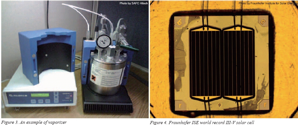
Achieving this objective requires devices with perfect epitaxial structures, as any imperfections will result in generation of heat that will reduce overall efficiency and cracks that will result in shorter product lifetimes. The use of vapor phase epitaxy deposition techniques offers a viable methodology to fabricate these highly complex structures in high volume provided sufficient control of the growth process is achieved. It is here that the precursor chemistry and product delivery is critical to the end result, both in terms of quality and cost.
Firstly, the purity of the chemicals employed must be extremely high to avoid contamination elements that can act as charge traps causing defects and degradation of performance. Many such elements are present in crude raw materials used in manufacturing processes, therefore, exceptional purification processes are needed to purify and reduce the level of certain ‘killer elements’ down to sub Parts Per Million (PPM). Fortunately, the III-V compound semiconductor industry employs these same chemicals, and precursor suppliers have been targeting ever purer materials for a number of years, so, the expertise already exists.
Secondly, the volume of chemicals needed to coat large areas in a commercially viable process presents a number of specific challenges related to the scale-up of these highly sensitive technologies. Increasing production capacity while maintaining product quality requires attention to detail at the microscopic level to ensure that the ‘fit for purpose’ status of the chemicals is retained for each upscale plant commissioned. With larger vessels and chemical reaction hazards entering unknown territory, thorough engineering assessments must be implemented. However, once running, the cost base for larger plants is appropriate for supply to the solar cell market. Building on the expertise gained from other electronic market areas enables precursor manufacturers such as SAFC Hitech to provide the correct quantities of the correct quality products to meet demand in an economical and acceptable manner.
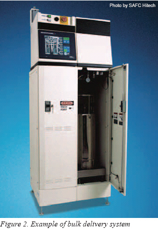
Focus on Delivery
 In order to achieve the most cost-effective processing, the most reliable delivery systems are needed. The introduction of chemicals to the deposition system must be performed in a fully controlled manner with no contamination in order for users to develop the most efficient methods to manufacture competitive products. SAFC Hitech has undertaken extensive research into all aspects of the precursor delivery technology needed to offer complete solutions for customer applications, and the delivery in bulk of the required precursors has been addressed using a variety of proprietary techniques. In order to achieve the most cost-effective processing, the most reliable delivery systems are needed. The introduction of chemicals to the deposition system must be performed in a fully controlled manner with no contamination in order for users to develop the most efficient methods to manufacture competitive products. SAFC Hitech has undertaken extensive research into all aspects of the precursor delivery technology needed to offer complete solutions for customer applications, and the delivery in bulk of the required precursors has been addressed using a variety of proprietary techniques.
Production of group III precursors, which employs SAFC Hitech’s unique adduct purification, have ensured high purity routes that can be scaled effectively to increase capacities. Robust chemistry has been combined with in-house plant engineering, resulting in per plant module capacities in the multi tonne per year range. These modules can be readily duplicated and may be deployed geographically as and where the market requirements dictate. Delivery tools are now available that allow users to handle large volumes of chemicals in a safe, controlled fashion, while the purity of materials remain unchanged from the reactor at the SAFC manufacturing site to the point of use at the customer site.
However, the role of the supplier does not end with isolation of the product as transportation to the customer and their usage must also be addressed by the containers utilized. Continuous design changes have allowed larger batches to be more efficiently used and transported to reduce waste and downtime, in turn, minimizing precursor impact on the economics of the end customer’s processes. Finally, fully depleted vessels must be treated and returned to service; hence, a complete product life cycle has been implemented to minimize environmental and commercial impacts. With the increasing implementation of various transportation and safety regulations on an international scale, logistic operations require dedicated experts in handling toxic and hazardous materials across oceans.
In summary, HBLED production is required to move to high volume manufacturing scales which are of a greater magnitude than ever before in order to realize the promise of economies of scale and ensure the widespread mass market penetration of HBLEDs in display and general illumination. Beyond existing companies looking to capture new markets, the PV and energy markets, in general, have attracted a flood of start-ups and new entrants, all keen to grab a piece of these economies. This is resulting in still more opportunities for chemical providers.
The potential for CPV devices to provide cost-effective solar cells in the short to medium term is high due to the advances in performance already demonstrated in III-V Multi Quantum Well (MQW) devices. The chemicals needed to fabricate these devices of necessity need to be of ultrahigh purity and available in high volume at low cost. Companies such as SAFC Hitech have made great strides forward with purification technologies to provide unparalleled starting material quality to the market in order to allow the highest performance structures to be grown. Furthermore, these companies’ commitment to capacity installation will result in lower cost precursors to effectively drive down end module prices.
Dr. Geoffrey J. Irvine joined Sigma-Aldrich, Corp. (www.safcglobal.com) as Product Line Specialist for Organometallics in August 2001. Irvine was quickly promoted to Product Line Manager for Organometallics with broader responsibilities in new product development and the overall product line strategy. In early 2003, Irvine moved to the SAFC business unit as Business Development Manager for the segment that would subsequently become SAFC Hitech. Promoted in mid 2005 to Director of Business Development, Irvine led the development and long-term strategy and revenue growth of SAFC Hitech. Irvine then served as Director of Marketing and Commercial Development for SAFC Hitech and in 2009, he moved into his current role at VP of Marketing and Business Development, SAFC Hitech. He holds an M.S. and Ph.D. in Organometallic Chemistry from the University of Auckland, graduating with honors.
For more information, please send your e-mails to pved@infothe.com.
ⓒ2011 www.interpv.net All rights reserved.
|


.jpg)