By Peter Weier
 Minimum demands on international competitiveness are high process safety, reliability, significantly reduced service intervals, low consumption costs and a most flexible integration into fully automatic cells. There is a high demand for innovative solutions in the process--and automation technology for silicon brick production and the thin-blade cutting technology belong to this. Minimum demands on international competitiveness are high process safety, reliability, significantly reduced service intervals, low consumption costs and a most flexible integration into fully automatic cells. There is a high demand for innovative solutions in the process--and automation technology for silicon brick production and the thin-blade cutting technology belong to this.
Photovoltaic Technology in Change
The international photovoltaic market undergoes a phenomenal market development. Presently the 30 gigawatt-mark in solar power capacity is exceeded. In the sustainability study ‘Solar industry--Entering new dimen-sions’. Swiss Bank Sarasin in Basel--which is well known for their solar expert reports--predicts increase average annual PV growth of 33% worldwide up to 2015. It is surprisingly positive to have so many new installations in a lot of markets this year, achieving a total of 13.8 GW.1) In the year 2009, Germany was scaling up to place one of the world’s largest solar markets. However, also the U.S., China and India are strongly catching up. For instance, China is planning to invest in alternative energies. Until the year 2020, the government of China has decided to extend their part at the total requirement energy to 16%. Planned capacities of individual Asian manufacturers of solar wafers, cells and modules are moving to the Gigawatt direction by realizing new production plants. A gigantic investment in new machines and cells is planned worldwide. With respect to the grid parity a change to process-optimized production can be strongly noticed.
Kerf Loss is not the Most Important Factor
Times have changed--silicon price per kilogram of US$500 is no longer up to date. This material is presently available at a price of approximately US$50 per kilogram on the spot market. For that reason, investments and the decision to purchase machines are made more independently of the prices for raw material, more important is the aspect of process optimization nowadays. The market is offering very different processes in processing silicon bricks. The spectrum of different cutting technologies varies from Outer Diameter (O.D.) cutting to band, wire and Inner Diameter (I.D.) cutting processes and now also thin-blade cutting methods are offered. Before making a decision which cutting machines shall be applied in future, it is advisable to compare not only the different processes of well-known but also the new methods of silicon brick production.
Starting with Sand--Getting a Wafer
Since the early beginning of the industrial photovoltaic production, not much has changed with respect to the core process of wafer production technology. However, there are various processing steps to get a finished wafer out of this raw material: sand. Dependent on the respective processing technique and also dependent on the silicon used, individual steps could vary.
The most efficient process is the Czochralski-method2) getting monocrystalline raw silicon ingots shaped like a cylinder which have to be processed later on. The first step is to cut end pieces (top and tail), then additionally a test wafer is cut with a thickness of approx. 1 to 2 mm for material--respectively, quality control. This process is called ‘cropping’. Afterwards raw ingots are cut into segments of 200 mm to 1,000 mm for further handling and processing.
Multicrystalline silicon, however, is melted in square crucibles in sizes which are applied presently of (length x width x depth; dimensions in millimeter) 878 x 878 x 480 (G5) and in dimensions which will be used in future of 1,050 x 1,010 x 550 (G6). Following the ‘crystallization’ process the raw silicon brick--also called ingot--is cut to square-shaped bricks on a band or wire saw to the standard wafer sizes (125 x 125 or 156 x 156 mm). After this process the lateral surfaces are ground, polished and--in the next processing step--the edges are chamfered. Sub surface damages, resulting of the above mentioned cutting process, are reduced significantly by this complex surface and edge processing step. The aim of this shall be to get maximum yield of each individual brick.
To check material quality and for the purpose of detection which means to localize possible impurities, there is done a resistance and lifetime measurement as well as an infrared-screening at each brick. After those measurements cropping or also top and tail cutting are done. This is done to cut off top and bottom part, respectively the cutting of silicon carbide inclusions in the silicon material of bricks. Those end pieces cannot be used for being processed to wafers because of their diminished conductivity. Inclusions in the center part of bricks are also cut out with this complex method in order to avoid a crack of wire during the wafering (slicing) process.
A crucial factor for the quality of final product: wafer, and for an effective production process, is an optimized production of the raw silicon ingots with high process safety.
Tradition with Future
The O.D. saw is one of the oldest cutting methods. Assembled with diamond cutting discs, this saw has been used industrially for decades for the cutting process of concrete, glass, ceramics, stones and metals. This cutting process excels by its simple and above all sturdy application, offering a maximum process stability. The cutting blade with the typical thickness of 3.5 mm is mounted on a working- respectively cutting spindle with clamping flanges. Feed motion during cutting process is done with the help of a driven cutting table or directly via cutting blade. Especially in the photovoltaic sector the work piece can be positioned in a simple prism rest, guaranteeing a tension-free cut without chipping.
The German Arnold Group belongs to the pioneers of this processing technique of brittle materials. In the early nineteen-eighties--then the first production cells for manufacturing wafers had been installed--they have modified and enhanced cutting machines based on the special requirements of silicon manufacturing customers. First cutting centers with automatic, robot-assisted working steps for loading and unloading purposes had been supplied in 1995. The inflationary price for silicon raised production costs due to high kerf loss caused by the cutting discs. This well-approved and nearly service-free O.D. saw nearly sank into oblivion. It had been pushed aside by other, sometimes significantly more expensive techniques, offering a lower consumption up to eightfold.
Accurate Cut
The Swiss company Meyer Burger already developed an I.D. saw for cutting wafers in the semi-conductor industry in the 1970s. Afterwards photovoltaic manufacturers have adopted this cutting process for expensive, brittle materials. Very impressive are those extremely precise cuts with very small cutting width of 0.5 mm and less. This very complex process is similar to a special circular saw technique. Approx. 7 minutes will be required for one cut in case of an ingot format of 156 x 156 mm. After an average number of 1,000 cuts the cutting blade must be exchanged manually. Mounting and dismounting including adjusting requires a period of several hours--even it is done by a very experienced worker. Tooling costs for a new cutting blade amount to at least 500 euros, net. And standstill of production shall not to be underestimated, which is caused by a regular--sometimes weekly--exchange of tools. This very exact process is linked with high investment costs and high tooling and servicing costs. Availability of machine declines to 70% due to those high standstill times required for the exchange of cutting discs.
Vertical and Horizontal Cutting
Numerous manufacturers are offering band saws for cutting silicon. This traditional technique roots in the processing of wood. A very famous manufacturer of band saws for cropping is--among other German companies--Jaespa, which is specialized in vertical machine executions for special materials. The Arnold-Group is offering a horizontal solution, especially suitable for cutting silicon. The guidances are specially encapsulated and thus protected against the very aggressive and highly abrasive water-silicon mixture. For cutting silicon the machines are equipped with galvanic cutting blades with diamond layers. In the optimized process the band saw passes the comparison with other methods. However, a great challenge is the band guidance which must be exchanged regularly due to its high wear of band. Experiences have shown that the lifetime of cutting blade is 20 m2, that means exchange of this tool after approx. 850 cuts. Although the exchange of blades and restart of operation could be done in a relatively short period of time, costs for sawing bands raise the operating costs considerably.
Additional Manual Work
In the years 2007/2008, the wire cropping saw appeared on the market which was a real alternative for the I.D. saw. Leading with this technology is the Swiss company HCT which had been incorporated by Applied Materials USA several years before. Cutting of silicon is done with the so-called slurry, a mixture of polyethylene glycol and silicon carbide, sticking at the cutting edge.
In the first step, up to 35 bricks are placed below the wire field of saw. In one working step, all tops and tails at the bricks are cut, that means 70 cuts are done simultaneously. This means processing time of wire saw technique is only half the time compared with processing time required for I.D. technique, however, a tremendous manual working time and expenses for extra works will be required. In principle this process is extremely inflexible due to the wire field fixed in the machine; this could lead to unnecessary waste of silicon. Set-up times for manual assembling and each cleaning step of cutting table require a lot of time. In case of a wire crash, the whole wire field of saw has to be recoiled completely, causing a high, time-intensive machine standstill and leading to long and expensive production downtimes. Taking all facts into consideration, also those extensive additional works including high auxiliary costs for cutting wire and slurry must be included in the calculation.
In recent times a lot of efforts have been done to realize the wire sawing process without slurry, only with a diamond covered wire. Taking first results into consideration the cutting speeds compared with the slurry cutting process are raised considerably. However, surface quality of wafers after the sawing process without using slurry varies significantly compared with the previous technique. This procedure--with or without slurry--is still very inflexible. Also the costs for diamond wire are worth mentioning. An automation, also an integration in an already automated production, is only possible with extremely high logistic expenditure.
Economical, Precise, Sturdy

Due to the new product generation of ‘thin-blade sawing technique’, the oldest cutting method--the O.D. cutting technique--is rediscovered for brick processing. This old and also new technique applied by the Arnold-Group is used for cropping of multi-crystalline silicon and also for cropping and squaring in the mono-crystalline brick processing. Manual, also semi-automatic and fully automatic working processes are possible.
The thin-blade sawing technique with the new designed guiding system for cutting discs (Photo 2), bases on the well-approved and known ‘circular sawing blade technique’, however, had been equipped with important advantages, allowing a cost-conscious brick production. Servicing and repairing costs are very low and the process stability and machine availability are very high with a minor requirement of manpower. The reduced consumption costs, the low costs required for energy, compressed air and above all the extremely low tooling costs make it possible to save an immense amount of money of up to 80% compared with the other sawing techniques.
While still cutting with a cutting blade thickness of 3.5 mm installed in the O.D. saw, the new thin-blade technology wins points with its extremely thin blade thickness of 1.5 mm; this means a maximum cutting width of 1.7 mm (Photo 3). The kerf loss is reduced by 50% using this thin cutting blade. This means cutting losses reduce on the basis of the today’s favourable silicon prices to about 2.50 euros per cut. Compared with conventional O.D. cutting saws working with a blade thickness of up to 4 mm in case of a kerf loss of up to 4.2 mm, the obtained savings have even more positive influence on the results achieved with the thin-blade cutting saw. Although there is still a kerf loss of silicon 2.6 times higher compared with the I.D. saws, calculating with the sawing surface of a wafer 156 x 156 mm (usual format), even noticeable cost savings could be achieved compared with other cutting techniques.
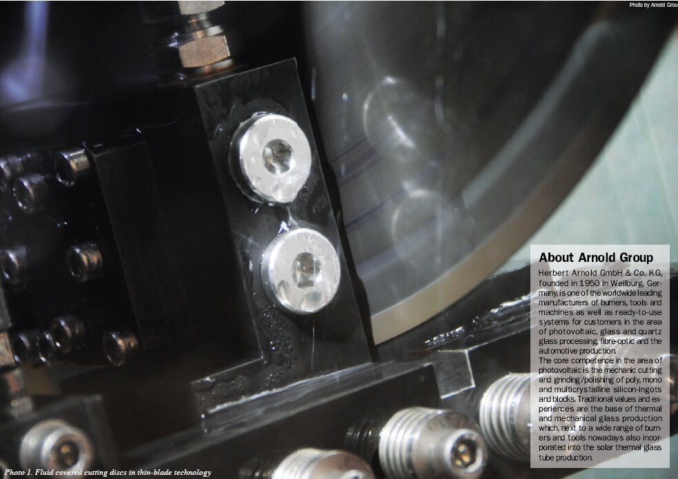
Having a look on the technical details will show the advantages of this sawing technique. The core point is the cutting disc, manufactured from a special tension-free and treated steel core of approx. 1.2 mm (Photo 1). Segments with a metal bound diamond concentration are soldered onto the edge of steel core. The hydrostatic fluid deposition takes care for an exact guidance of initial cut and avoids oscillations and flutters. This fluid deposition moves downwards together with the vertical travel of cutting disc and cares for an extremely precise cutting with a maximum tolerance of angularity smaller 0.1 degree. Layer height of cutting disc is 6.5 mm and is calculated for approx. 10,000 up to 15,000 cuts. Exchange of cutting blade requires a max. period of half an hour. Even in case of continuous operation the tightest tolerances required by the industry with respect to parallelism smaller 0.2 mm and angularity smaller 0.3 mm for a standard wafer format of 156 x 156 mm will be met.
Fully Automatic Process Sequence
The thin-blade sawing technique in the sector of cropping multicrystalline silicon has established itself on the international market. New machines with thin-blade sawing technique for cropping and squaring of monocrystalline silicon are offering further applications with fully automatic functions and are offering a lot of saving potential. The concept of the new thin-blade sawing technique for cropping of monocrystalline ingots allows a processing of round (150 up to 210 mm diameter) or squared (maximum 160 x 160 mm) ingots up to a maximum tube length of 2,500 mm. With the respective squaring machine silicon bricks respectively ingots as grown in a diameter range of 155 up to 220 mm could be processed. Here it is possible to process several ingot segments or individual segments up to a length of 2,500 mm either in a single cut process or in a batch cut process.
Single Cut Process or Batch Cut Process
 In a lot of regions worldwide the squaring of monocrystalline ingots is only done at individual ingot segments--Single Cut Process (SCP), however with the new machine generation of thin-blade cutting saws a forgotten processing possibility enters again in the market called Batch Cut Process (BCP). 10 years ago this process had been done with thick cutting discs and is now gaining attractiveness again. In this BCP up to five ingot segments could be placed, one behind the other, and are processed in one working step. The BCP allows a higher throughput which does not only excel by time savings but is also financially profitable. Production costs could be reduced by about 30% compared with established processes. Due to the higher throughput of those machines with two in parallel working cutting discs also investment costs and above all consumption and tooling costs could be reduced significantly. In a lot of regions worldwide the squaring of monocrystalline ingots is only done at individual ingot segments--Single Cut Process (SCP), however with the new machine generation of thin-blade cutting saws a forgotten processing possibility enters again in the market called Batch Cut Process (BCP). 10 years ago this process had been done with thick cutting discs and is now gaining attractiveness again. In this BCP up to five ingot segments could be placed, one behind the other, and are processed in one working step. The BCP allows a higher throughput which does not only excel by time savings but is also financially profitable. Production costs could be reduced by about 30% compared with established processes. Due to the higher throughput of those machines with two in parallel working cutting discs also investment costs and above all consumption and tooling costs could be reduced significantly.
As an example: squaring of five work pieces in the BCP, entire moving way, that means the addition of cutting disc radius + cutting stroke + 5 x work piece length + overflow is 3,246 mm. Radius of thin-blade cutting discs (in case of a diameter of 700 mm) = 350 mm, cutting stroke = 10 mm, five work pieces with each 500 mm = 2,500 mm with each intermediate distance for clamping system of 94 mm = 376 mm and the overflow of 10 mm. In the SPC the total moving way is calculated of radius of cutting disc + cutting stroke + 1 x work piece length + overflow with 870 mm. In case the same feed rate is used of 25 mm per minute, the result in case of SCP will be an average processing time of 80 minutes per length of segment compared with the BCP of 56 minutes per length of segment. The manufacturer calculates with a time advantage of the BCP of 24 minutes per segment.
If we only consider the example of five work pieces, it is easy to calculate which reductions of moving ways and which time savings could be achieved and are possible--taking the high production throughput into consideration with the help of this new process. Furthermore, this example shows the high potential of cost savings.
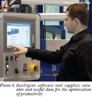
Without Control--No Efficiency
A cost-efficient production is no longer realizable without software-controlled process control in real time. The Arnold-Group has developed an intelligent and presently worldwide the only available software tool Arpat (Photo 4). This tool collects, analyzes, stores and visualizes adjustments, consumption and capacity data also of machines with thin-blade cutting technique. All parameters could be inspected via touch panel PC and can be changed any time. Collected data of several processes can be compared with each other. The protocol can be printed and passed on to a higher-ranking manufacturing execution system (MES).
The thin-blade cutting technique is already approved as competitive, innovative, alternatively compared with the other processes available on the market. All machines, for cropping of multi-crystalline silicon and also for cropping and squaring of mono crystalline silicon are constructed and designed for the volume market with high degree of automation. However, they are also a very good solution for companies with medium-sized or smaller production capacities. The thin-blade cutting machines can be integrated any time--also at a later date--into automated production cells, where, for instance, robots are doing the loading and unloading of bricks and the optimum positioning within the machine. The technique is easy to understand and the operation does not require a lot of training or even additional education. In view of the gigantic increase to gigawatt production lines, new ways to process silicon are required. The thin-blade sawing technique has already gained a safe place on the market despite changed market conditions.
Peter Weier is Head of the business unit silicon processing and automation of the Arnold-Group (www.arnold-gruppe.de). This company is offering process and automation technology for the wide spectrum of silicon brick processing with core competence: mechanical cutting, grinding and polishing, everything from one supplier. Weier had gained 20 years in international project experiences on the sectors quartz glass- and glass fibre industry; in 1995, he started with the main focus on photovoltaic and he is significantly involved in concepts, developments and sales of machines for glass-, quartz glass- and silicon processing.
REFERENCES
1) Solar industry--Entering new dimensions, November 2010, Bank Sarasin & Co. Ltd., Basel/Schweiz; http://www.sarasin.ch
2) Czochralski-process: http://www.uni-stuttgart.de/izfm/lehre/Werk_Her.pdf
For more information, please send your e-mails to pved@infothe.com.
ⓒ2011 www.interpv.net All rights reserved.
|


.jpg)