By Dr. Samuel Kim
.jpg)
The solar industry is set to be transformed by nanotechnology as companies with new inking techniques work to lower overall solar cell costs by more than 25% and preserve solar as one of the leading renewable energy options in the market for decades to come. Solar must remain cost competitive in the coming years if it is going to compete with energy technologies like wind, nuclear, and coal, especially in light of the coming expiration of federal tax subsidies and credits for solar installations.
One of the keys to increasing solar’s competitiveness is to draw down the costs of production. The U.S. Energy Information Administration recently concluded that the ‘cost of generation’ (in US$/MWh) of solar PV will make it 2 times as expensive as wind, more than 3 times as expensive as nuclear, and slightly less than 4 times as expensive as conventional coal by 2016.1) New innovations and technologies will be necessary for solar PV-based approaches to lower the cost enough to be competitive with other competing technologies. The U.S. Department of Energy is also looking to fund new innovations that it believes will make the costs of solar PV more competitive and recently awarded Applied Nanotech Holdings, Inc., a U.S. nanotechnology company, a grant in the amount of US$1.6 million to establish a pilot production facility to manufacture and commercialize proprietary ink materials for the application of metallic conductor layers on thin silicon solar cells.
Taking into account only the solar cell itself, there are two main ways to lower the cost of energy generation: 1) make more efficient solar cells, or 2) lower the cost to make them. As silicon is the largest cost in conventional solar cell production, making up 50%-60% of the overall cost, it is pivotal that costs associated with its use be lowered. Ink technologies based on nanotechnologies enable ultra-thin silicon wafers to be used for photovoltaic applications. By reducing the amount of silicon used, the cost of solar energy can be lowered dramatically.
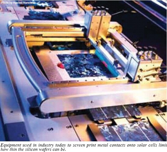
Currently, solar cell wafers must be thick enough to survive the direct contact metallization processes. Industry standard solar cell manufacturing processes use screen printing equipment which directly contacts the wafer and can exert enough force to cause breakage for thin wafers. If metallization could be done without touching the wafer, it would allow for silicon solar cell wafers to be much thinner than they are today, which could reduce the overall cost of the device. Non-contact print techniques like the inkjet technologies employed by Applied Nanotech provide a route to realize thin-silicon wafer technology in a high throughput production environment.
How Non-contact Printing Lowers Silicon Costs
Using methods such as inkjet, aerosol jet, and spray coating--all non-contact methods--offers several important advantages over traditional manufacturing approaches.
Silicon Costs
Companies can save substantial costs on the amount of silicon used by enabling the use of thinner wafers; screen printing requires thicker wafers due to the mechanical pressure exerted onto the wafers during the printing process.
Processing Flexibility
Multiple different metals (or other materials) can be printed simultaneously without having to dry or fire the wafer between steps; with screen printing, one metal must be patterned, dried, fired, and then the next metal can be printed due to the fact that the screen touches the substrate and can cause the previously printed pattern to be smeared or otherwise corrupted.
Higher Resolution
Narrower metal lines can be printed reducing shadowing effects, which increases the efficiencies of solar cells; screen printers are not able to achieve the fine resolution of inkjet and other non-contact printing technologies and thus more sunlight can be blocked by the wider lines.
Increased Efficiency
The use of thinner silicon wafers reduces the distance electrons and holes must travel to the electrodes, allowing for more efficient extraction of electricity from the solar cell.
Ink Costs
Non-contact printing approaches such as inkjet and aerosol jet are drop on demand printing techniques which efficiently places ink only where it is required; screen printing is much less efficient due to wasted ink on the screens, squeegees, and other printer components which must be cleaned.
Collectively, these process changes translate to a cost savings of ~44%, or overall solar cell cost savings of ~27%. These improvements have the industry excited at the potential to save significantly on raw materials costs.
Other nanotechnology methods used by Applied Nanotech could result in solar cell efficiency improvements as well. While traditional silicon wafers need to be ~180 microns thick, the methods used by Applied Nanotech bring that down to 100 microns and below. Since these inking formulations have a high conductivity, the result is equivalent performance using 30% less ink when compared to competing screen printed pastes.
Making the Transition Easy for Customers
Aluminum is entrenched in the silicon solar cell market, especially for backside contacts, so getting clients to think differently about how products are made can be challenging. To make this transition smoother, Applied Nanotech is also producing screen printable aluminum pastes that have similar properties as the non-contact printable ink formulations. This gives solar cell manufacturers the ability to try the material in paste form on their existing solar cell lines, before fully transitioning to a non-contact printable approach. Once solar cell manufacturers are comfortable with the pastes, replacing screen printed aluminum with a non-contact printed aluminum is easier than changing to an entirely new metal or processing system.
Similarly with silver, which is currently the industry standard for front side metal contacts, screen printing can be transitioned to non-contact printing methods. With a non-contact printable silver ink formulation, these methods allow manufacturers to replace the silver pastes used traditionally with many technical and cost advantages. Printing high resolution narrow lines is important for this application since it is on the side of the cell facing the sun. But by using precision ink printing, Applied Nanotech is able to achieve higher performance and higher efficiencies while using less silver ink.
Aluminum and silver aren’t the only metals being used with Applied Nanotech’s inking technologies. Though not as popular as these two, nickel and copper are now being used by companies looking at next generation architectures of solar cells which could potentially make a significant impact in the future. Partnering with these companies, Applied Nanotech hopes to make big inroads into this area as well.
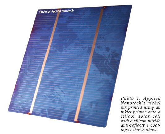
Nickel ink formulations have applications for barrier layers for subsequent plating and/or patterning of other metals on top. Nickel prevents metals that diffuse quickly into silicon, such as copper, from destroying the electronic structure of the solar cell. By contrast, Applied Nanotech’s techniques allow them to achieve very good printability, adhesion, and electrical characteristics. A sample of Applied Nanotech’s nickel ink which has been printed using an inkjet printer onto a standard silicon solar cell wafer with a silicon nitride antireflective coating is shown in Photo 1.
Copper is of high interest to replace silver contacts because of the large difference in cost. Copper ink can be used together with nickel inks to print front side contact for solar cells as a replacement for silver front side contacts. Currently copper is plated on top of nickel which can be an expensive and time consuming process.
When nanotechnologies are applied to solar’s cost problems, the ideas that result are game-changing. Many other opportunities exist as well. Applied Nanotech is currently working on developing non-contact printable p-type and n-type dopants. These inks will enable printing equipment to be leveraged for more manufacturing steps, further reducing the cost to manufacture the cell by using non-contact printing technologies. Looks like a bright future for solar, thanks to nanotechnology.
Dr. Samuel Kim, Ph.D., is Vice President of Business Development for Applied Nanotech, Inc. Its holding company, Applied Nanotech Holdings, Inc., a U.S. listed company trading under the stock symbol APNT, is a research and commercialization company focused on solving problems at the molecular level.
REFERENCES
1) US Energy Information Administration, ‘Annual Energy Outlook 2010,’ released May 11, 2010
For more information, please send your e-mails to pved@infothe.com.
ⓒ2010 www.interpv.net All rights reserved.


.jpg)