By Els Parton, Johan van der Heide, Giovanni Flamand, Jef Poortmans
.jpg)
No Heat to Waste
As classical photovoltaic systems use photons originated by the sun, Thermophotovoltaic (TPV) systems use photons emitted by a heat source to generate electricity. For example, combustion systems in industry can act as heat source. In this way, waste heat produced during glass or steel production can be turned into electricity. Also consumer applications can benefit from TPV cells. Just think of domestic heating systems producing warm water.
Although TPV systems have a huge potential in terms of industrial and consumer applications, they have not yet made it to the market. The most important reason for this is the complexity and large cost of the systems.
Germanium-based TPV Cells
A TPV system typically consists of a heat source heating up a selective emitter. This, in turn, radiates photons in a relatively narrow wavelength band which are then absorbed by TPV cells (see Figure 1). The emission peak of selective emitters typically used in TPV systems is close to the bandgap of germanium. Therefore, germanium photovoltaic devices are well suited as TPV cells. Moreover, this semiconductor has a relatively low cost as compared to other TPV materials such as InGaAs or GaSb.
An important theme of the TPV research community is cost reduction. For germanium-based TPV cells, excellent results were obtained demonstrating both cost reduction and improved conversion efficiency. The approach and the results are described below.

Low-cost Process Flow
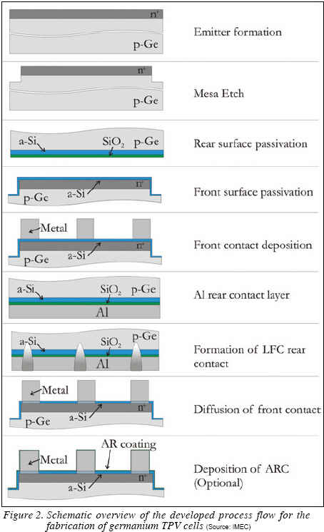
A first step towards more cost-effective germanium TPV cells was the development of a process flow for cell fabrication using low-cost processing techniques which are industry applicable (Figure 2).
Emitter Formation
On a p-type germanium substrate, an n+-emitter is made by diffusion of phosphorous from a spin-on dopant which is applied by spin coating. Next, the active cell area is patterned using standard lithography and wet chemical etching.
Passivation
Passivation is next. Amorphous silicon is used to passivate the surface since this is an excellent passivation material for germanium. An amorphous silicon layer is first grown on the front surface, directly followed by a layer on the rear. The layer thickness on the front is less then on the rear to minimize absorption of photons in the amorphous silicon layer itself.
Optical Confinement
Optical confinement is very important in TPV cells because the absorption depth of the majority of the incoming photons is close to the thickness of the germanium substrate. Keeping in mind that the classical aluminum rear contact has a very low reflectivity, it is important to optimize this structure. This was done by combining the aluminum contact layer with the amorphous silicon passivation layer and a silicon dioxide layer. This stack shows very good reflectance properties. The silicon dioxide layer was grown at the same temperature as the amorphous silicon since a higher temperature decreases the passivating quality of the amorphous silicon.
Rear Contact Formation
Since amorphous silicon is a poor conductor, contact between the aluminum contact layer and the base has to be made in a next step. This was done using a laser to locally heat the aluminum layer. Because aluminum locally creates a p-type doping around the contacted area, the full rear side is passivated.
Front Contact Formation
For the front contact, a stack containing palladium and silver is deposited on the amorphous silicon passivation layer. The contacts are realized in a subsequent annealing step in which the palladium diffuses through the poor-conducting amorphous silicon layer.
Germanium TPV Cells on Substrates with an Optimized Surface Finishing
The process flow mentioned above, doesn’t involve any epitaxy and this opens doors to further cost reduction of the fabricated TPV cells.
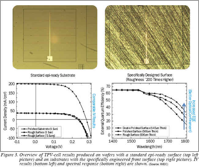
Today, germanium-based TPV cells are made using mirror-polished epi-ready substrates, enabling the epitaxy-based process flow typically used for the realization of high-efficiency multi-junction solar cells. In the new approach, specifically designed substrates with relaxed surface-finishing conditions were used which are more cost-effective than the ones with an excellent smooth front surface finishing.
Of course, the use of these novel germanium substrates holds some challenges. It has an impact on the emitter formation and the contact realization.
Optimization of the Emitter Formation
The spin-on emitter formation has to be optimized in order to prevent any interruptions in the spin-on dopant layer on the front surface. Because the emitter is formed by diffusion from phosphorous from the spin-on dopant, non-covered parts would immediately lead to an emitter-less area. When a metal contact is deposited on such an area, a direct contact is created to the base, causing a shunted cell.
This problem was solved in two ways. The first adjustment was to choose a spin-on dopant with a higher phosphorous concentration. This leads to a deeper emitter. This, and the fact that the phosphorous also laterally diffuses into the substrate, reduces the risk of interruptions in the emitter. The second adjustment was to use a lower spin-speed with which the spin-on dopant is deposited onto the substrate. This additionally prevents the formation of an open area, even at the spots with the highest roughness.
Where a deeper emitter would automatically lead to a decrease of the cell performance for standard photovoltaic cells, for TPV cells this effect is not as strong because of the spectral distribution of typical TPV systems. The TPV spectrum contains mostly long-wavelength, low energetic, photons which are absorbed deeply in the substrate far away from the emitter area.
Impact on the Contact Realization
Because of the roughness of the rear surface, this will not be fully covered by the thin layer of amorphous silicon. This leads to contacts even without applying Laser-fired Contacts (LFC).
The need for a subsequent LFC process strongly depends on the final application and the generated current in the cell. If high currents will be generated in the cell, a denser LFC contact pattern is required to reduce the rear contact resistance.
The situation on the front side is somewhat different. Because of the smaller contact area, the subsequent annealing step is always required.
Higher Efficiency, Lower Price
Germanium TPV cells using these specifically designed germanium substrates were manufacturerd and tested. Comparable IV results as with epi-ready susbtrates were measured. Also, an increased quantum efficiency was measured at long wavelengths (see Figure 3). This is due to an improved optical confinement in the newly developed cells.
TPV cells have been realized on substrates with relaxed surface finishing conditions, giving comparable performance as cells made on substrates with a polished surface. The associated cost reduction of the cells is an important aspect for the application of these germanium receiver cells in TPV applications.
Els Parton received her engineering degree and Ph.D. in Biological Sciences at the Katholieke Universiteit Leuven (K.U.Leuven), Belgium. She joined IMEC (www.imec.be) in 2001 as a scientific editor and is jointly responsible for authoring and editing the research organization’s numerous company technical documents and publications.
Johan van der Heide studied at the Rijksuniversiteit in Groningen, the Netherlands, and received his Master degree in Applied Physics in 2003. During his doctoral research at IMEC, Leuven, Belgium, he focused on the development of cost-efficient thermophotovoltaic cells based on germanium substrates. His research was funded by a personal fellowship of the Institute for the Promotion of Innovation through Science and Technology in Flanders (IWT-Vlaanderen) and was completed in 2009.
Giovanni Flamand received the M. Sc. degree in Physics Engineering and Ph.D. degree in Applied Sciences from the University of Gent, Belgium, in 1995 and 2000 respectively. Since 2000, he is working on the subject of III-V/Ge based high-efficiency photovoltaic cells. He is currently heading the High Flux Devices team within IMEC’s Solar Cell Technologies group, with as main research interests mechanically stacked multijunction solar cells for concentrator applications, and Ge-based thermophotovoltaic cells. He has authored or co-authored more than 60 scientific publications.
Jef Poortmans received his degree in Electronic Engineering from the Katholieke Universiteit of Leuven, Belgium, in 1985. He joined IMEC and received his Ph.D. degree in June 1993. Afterwards, he joined the photovoltaics group, where he became responsible for the group Advanced Solar Cells. Within this frame he started up the activity about thin-film crystalline Si solar cells at IMEC and he has been coordinating several European Projects in this domain during the 4th and 5th European Framework Program. In 2003, he became Cluster Coordinator of European Projects in the latter domain. In 1998 he initiated the activity on organic solar cells at IMEC which was complemented with an activity on III-V solar cells started in 2000. At the moment he is Program Director of the Strategic Program SOLAR+ at IMEC. This Program comprises all the photovoltaic technology development activities within IMEC.
For more information, please send your e-mails to pved@infothe.com.
ⓒ2010 www.interpv.net All rights reserved. |


.jpg)