By W. McMillan, T. Trupke, J. Weber, M. Wagner, U. Mareck, Y.C. Chou, J. Wong
In current solar cell manufacturing, incoming wafer quality is primarily determined by physical metrics, such as dimension, thickness, cracks, chips and by limited electrical parameters such as the bulk resistivity. Spatially averaged values or line scans of the surface limited effective minority carrier lifetime are also sometimes measured.
While the measurement of these physical metrics is important to ensure wafers are handled correctly by automated equipment, and in order to minimize breakage rate, they do not qualify a wafer in terms of its solar cell efficiency entitlement. Surface limited effective lifetime provides only very limited information on wafer quality due to, one, the strong influence of surface recombination on the measured data and, two, the fact this is an area-averaged measurement which is influenced by features that do not correlate strongly with cell performance, as will be explained later in this paper.
In this work, we introduce metrics that are derived from relative intensity variations observed in megapixel Photoluminescence (PL) images taken on as-cut multicrystalline silicon wafers. These metrics are shown to correlate with finished cell electrical parameters such as the open circuit voltage and the short circuit current density. In addition improved photoluminescence imaging equipment is described that allows megapixel PL images to be measured and processed at line speed in production.
Combining these improved hardware and software capabilities with the correlation metrics of cell performance data allows wafer and cell manufacturers to determine an efficiency entitlement for as-cut multicrystalline wafers.
Background
Surface Limited Effective Lifetime
The maximum value of the minority carrier lifetime of an unpassivated as-cut silicon wafer that can be measured by any technique is limited by surface recombination. Above this surface-limited value, the measured ‘effective’ lifetime has only limited correlation to the bulk lifetime, which is the value that is more useful in predicting cell efficiency. Another way of stating this is that there is a large range of wafers, all with differing bulk lifetimes, that will result in cells of widely differing efficiencies, for which the effective lifetime, as measured, appears almost identical (and is the surface limited lifetime value).
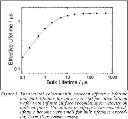
This issue can be explained by reference to Figure 1, which shows a theoretically predicted variation of effective lifetime with bulk lifetime, for a 200 micrometer thick silicon wafer. With increasing bulk lifetime, the effective lifetime (τeff) converges towards a constant value, which is given as 2)
Equation 1 assumes uniform photogeneration and steady state measurement conditions, with W the wafer thickness and Dn the electron diffusion constant. For a p-type wafer Equation 1 predicts a value of τeff= 1.3 μs. This saturation value depends on the measurement conditions, for example for transient lifetime measurements the value of ‘12’ in Equation 1 must be replaced by 2, resulting in τeff= 1.5 μs2). Taking such variations into account the theoretical correlation between bulk lifetime and effective lifetime shown in Figure 1 in principle allows conversion of measured effective lifetime into estimated bulk lifetime3), 4). An important point to be noted from Figure 1 is that variations in measured effective lifetime become very small for bulk lifetime values exceeding τeff= 10 μs. As a result even small experimental errors in the measured effective lifetime will results in large errors in the estimated bulk lifetime data and effective lifetime becomes essentially non-predictive for bulk lifetime and, therefore cell efficiency. A recent study by Haunschild et al5) concluded that average effective lifetime is therefore not a reliable parameter to predict cell performance, and at a first level, this is due to the saturation of the effective lifetime as discussed.

This saturation effect was confirmed experimentally in a recent experimental study by some of the authors of this paper. This work compared the doping-normalized area averaged PL intensity from PL images and the area averaged μ-PCD lifetime measured on multicrystalline as-cut wafers, from different positions within the same silicon brick1). Figure 2 shows data from that study. Low average PL intensity and reduced average lifetime are observed near the bottom and top regions, respectively of the brick. Very little variation in both quantities is observed however in the centre part of the brick, where both the average lifetime and the average PL signal are dominated by surface recombination; in this region there are in fact large variations of inherent wafer quality, and specifically average bulk lifetime and spatially resolved features that impact this value. Information about wafer quality can therefore only be gained from spatially averaged quantities for very impure wafers near the top- and bottom regions of the brick.
A benefit of the relationship between bulk lifetime and effective lifetime as shown in Figure 1 is that only the areas with the lowest bulk lifetime have an impact on the measured effective lifetime. Only the poorest quality regions of a wafer are therefore expected to give significant contrast in spatially resolved lifetime measurements on unpassivated wafers, an aspect that is exploited in PL imaging as explained below.
Finally, even if it were possible to measure average bulk lifetimes on unpassivated wafers, this measurement can will not perfectly correlate with final cell efficiencies. The reason for this is that the average bulk lifetime is affected by many factors, such as impurities, dislocations, grain boundaries and the like. In cell processing the impact of some of these can be almost entirely removed, for example via gettering and passivation, whereas the influence of others cannot. As discussed below, in order to determine a good predictor of the impact of wafer quality on cell efficiency one must determine spatially resolved lifetime features, and, further, one must discriminate between those of these features that are removed during processing of wafers into cells and those that are not.
Photoluminescence Image Interpretation
Photoluminescence (PL) imaging is a fast method to provide spatially resolved effective minority carrier lifetime data on silicon wafers6). The ability to measure high resolution PL images on as-cut silicon wafers has been demonstrated in previous studies7).
The concept behind the use of PL images for quality control on as-cut wafers is that areas of strongly reduced bulk lifetime are associated with specific types of recombination active sites and therefore appear in PL images with characteristic spatial patterns of reduced luminescence intensity. Application of specialized automated image processing and pattern recognition techniques allow the quantity and quality of the individual recombination sites to be derived, which can then be correlated with cell electrical parameters. An example of such correlation was recently given by Haunschild et al, who demonstrated correlations between cell Voc data and the area density of dislocation networks and also statistical variations in Voc between centre-, edge- and corner wafers5), 8).
An automated BT Imaging production PL imaging system (model iLS-W1TM) was used for the experiments in this study. The system allows megapixel PL images to be taken with homogeneous monochromatic laser excitation on multicrystalline silicon wafers with a size of 156 mm x 156 mm. An advantage of the iLS-W1TM system is that it has been designed for inline use during production, and is capable of a throughput of 2400 wafers per hour, allowing large quantities of wafers to be inspected quickly.
On unpassivated silicon wafers the luminescence quantum efficiency, i.e. the number of luminescence photons per incident photon is extremely low, typically on the order of or even below 10-8, which results in several experimental challenges when it comes to taking high resolution PL images at line speed.
Firstly, sophisticated optical filtering is required for a sufficient separation of reflected excitation light from the measured signal. If there is insufficient optical filtering this results in excitation light contributing to the measured luminescence image, which in turn requires image corrections using a combinations of PL imaging with conventional optical images9). The BT Imaging iLS-W1TM PL imaging system uses highly specialized optical filtering arrangements and thereby avoids such illumination artifacts altogether.
A second challenge for inline PL Imaging of unpassivated silicon wafers is in the required sample throughput, which reduces the available acquisition time to one second or less. In previous PL imaging studies measurement times of typically 60 seconds were reported for megapixel PL images on as-cut wafers5). The BT Imaging iLS-W1TM incorporates an advanced PL imaging technology, which uses optimized illumination and detection sub-systems in order to reduce image acquisition time for as-cut wafers to under 1s without compromising image quality or spatial resolution.
In addition, the BT Imaging system incorporates proprietary image processing algorithms which can be used to determine key metrics of the wafers, and thus enable real-time sorting of the wafers into quality bins at line speeds of around 2,400 wph.
In a first trial reported in this work, multicrystalline wafers from the bottom to the top of a cast boron doped silicon brick were analyzed. PL images were performed on every tenth wafer from the brick, and sister wafers (wafers next to the samples that were used for PL imaging) were processed into industrial screen printed solar cells. PL images were analyzed for electrical defects with the automated image processing algorithms developed at BT Imaging. These algorithms identify specific defects related to decorated dislocations and grain boundaries, and also regions with increased atomic defect density in wafers from the top and bottom regions or from edge and corner regions within the ingot.
In a second trial, PL images of 5000 wafers were measured. These wafers were a mixture of wafers from several suppliers. The wafers were then shipped to a solar cell manufacturer for processing into screen printed solar cells.
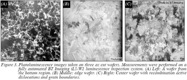
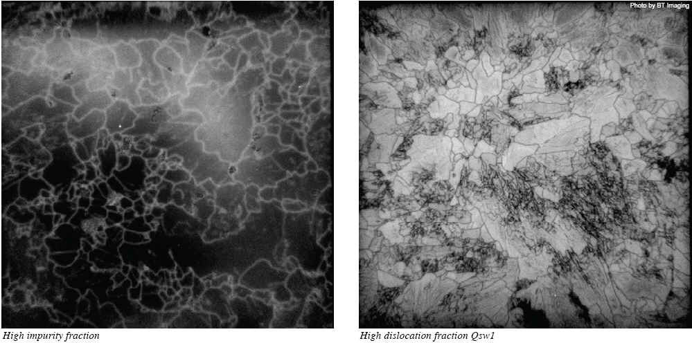
Three typical examples of PL images of as-cut wafers that are representative of the features seen in the wafers used in this study are shown in Figure 3 The image at the top (Figure 3A) shows a wafer from the near bottom region of the ingot. The contrast inversion that is observed, where the sample is generally dark, but where grain boundaries and dislocations appears lighter, is caused by internal gettering of impurities in the local regions surrounding the grain boundaries and dislocation networks5). The generally dark appearance of the wafer is caused by high distributed atomic defect concentration, which results in low luminescence signal across the wafer. This wafer is typical of samples from the bottom and top regions of silicon bricks, data for which is circled on the far left hand side in Figure 2.
Figure 3B shows an image of an edge wafer with reduced effective lifetime near the right hand side. The severity and area fraction of that area can be assessed based on PL images5).
Figure 3C shows an image of a wafer with a high density of local defects. These are caused by recombination active grain boundaries and dislocation networks, formed during casting of the block.
Dislocations and Grain Boundaries
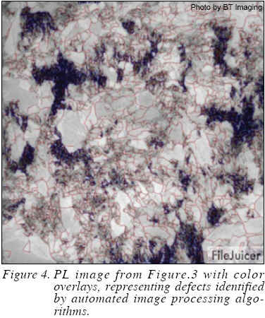
The BT Imaging image processing algorithms identify and distinguish different types of defects that appear in as cut wafer images with specific contrast, patterns or spatial frequencies. Figure 4 shows the PL image of the sample in Figure 3C, however with added color overlay for two specific types of defects. The algorithm provides the area density of those defects, which can then be compared to cell efficiency data.
Figure 5 shows the correlation between relative cell IV data (Voc, Isc, efficiency) and a specific defect metric that reports the area density of recombination active dislocation clusters. Note that this metric is quite different from previous techniques that used specifically prepared chemically etched samples, where physical dislocation density is measured from counting etch pits with a photographic scanner.
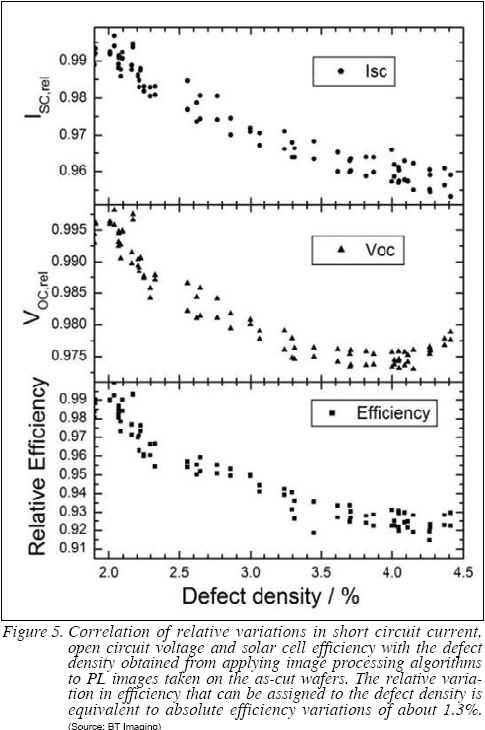
In Figure 5 a clear trend of reduced cell performance can unambiguously be assigned to the increase in defect density as measured by the BT Imaging PL Imaging system. Importantly, this shows that these specific type of defects are already present as recombination active centres in the as-cut wafers and remain as efficiency limiting defects in the finished cell.
The observed relative variation of 2.5% in Voc is equivalent to about 15mV absolute, and in good agreement with results from an earlier similar study5). The main impact of the dislocation density is on Isc with relative variation of 4.5% that can be assigned to the defect density variation. An 8% relative efficiency variation can be assigned to the defect density variation, which is equivalent to a ~1.3% absolute efficiency variation for typical industrial cells with an average efficiency of 16%.
Regions with High Impurity Concentration
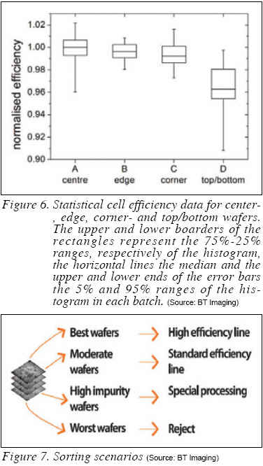
In the PL Imaging study of 5,000 wafers, the PL images were grouped into four categories: i) centre wafers, ii) edge wafers with one low lifetime edge, iii) corner wafers with two low lifetime edges and iv) top- or bottom wafers. IV data of the cells were statistically analysed separately for each group. First, a consideration of the impurities is highlighted by the data shown in Figure 6 This is the statistical cell efficiency data for the four categories of wafers listed above. The median values show the highest efficiency for the centre wafers, as expected. Relatively small reductions in median cell efficiency of 0.06% are observed for edge wafers and 0.12 % for corner wafers. These variations are smaller than in a previous study, where 0.2% and 0.3% absolute efficiency losses were reported for edge- and corner wafers, respectively 5). We note that edge and corner wafers often have higher impurity levels (that can partially removed in processing), and the effect of these impurities can be offset by lower levels of dislocations The strongest impact on cell performance and the largest statistical variation within each batch was observed on bottom/ and top wafers, which are the most impure, and for which a 0.6% absolute efficiency reduction is observed.
Another example of the correlation between defect density as measured on as-cut wafers and cell efficiency is shown in Figure 6 for a larger sample set. In this Figure, a strong correlation between the levels of recombination centers (as detected by the BT imaging PL Imaging system) and ultimate cell efficiency can be observed. This result is in line with the results of the previous study reported in Figure 5.
The correlations between cell performance and metrics derived from measurements on as-cut wafers discussed here depend strongly on the cell process and its ability to reduce the impact of specific defects on cell performance via gettering and passivation. The lower than expected correlation with edge/corner effects reported above shows for instance that the specific cell process used in this trial appears to be particularly efficient in terms of gettering distributed atomic impurities from the edge and corner regions. That data is also an example for the impact of gettering on the correlation between bulk lifetime in the as-cut wafer and the final cell performance.
Practical Application
There are several potential applications of the methodology outlined above.
Identifying Poor Quality Wafers Which Should Not Be Processed into Cells
In the iLS-W1TM application software, users can set a quality threshold below which poor wafers are rejected. The iLS-W1TM can then quickly identify wafers which would produce poor performing cells and which can be rejected back to wafer suppliers.
Identifying the Highest Performing Wafers Which Can Be Used in High Efficiency Cell Lines
In the iLS-W1 application software, users can easily set a quality threshold above which the best wafers are identified. Since high efficiency cell lines employ higher cost cell processing techniques to increase the cell performance it is logical to use the highest quality wafers to ensure the maximum benefit of the extra cost is achieved. Also, with increasing cell efficiency the impact of the defect density on cell performance is expected to increase over the correlations discussed above for conventional screen printed cells. Sending the best wafers to the high efficiency lines will, therefore, increase average efficiency across lines in production.
Sorting Wafers into Bins for Optimized Processing
As discussed in this article, the electrical impact of specific defects can be modulated by the cell processing techniques employed. For example, users can sort wafers with high levels of distributed impurities (edge/corner wafers) which can then be processed with tuned cell processing, e.g. increased gettering, to increase the cell performance. This method allows cell makers to gain a competitive advantage by employing their internal cell processing know-how.
Wafer Manufacture Process Optimization
In addition to being a quality control metric, the data is valuable for process improvement and optimization. Ingot casting is a critical process which essentially determines the level of impurities and local defects which are present in the wafers. The wafer data can be used to optimize the casting process to minimize defects and reduce cost. This will become more important as faster and/or larger casting is trialed and brought to production.
Cell Process Optimization
The wide distribution of defect densities present in industrial multicrystalline wafers results in a wide distribution in cell performance data as seen for example in Figure 5. Cell process optimization is greatly facilitated by using wafers with a narrower distribution of defect densities. This can be achieved by presorting wafers into different bins using the iLS-W1
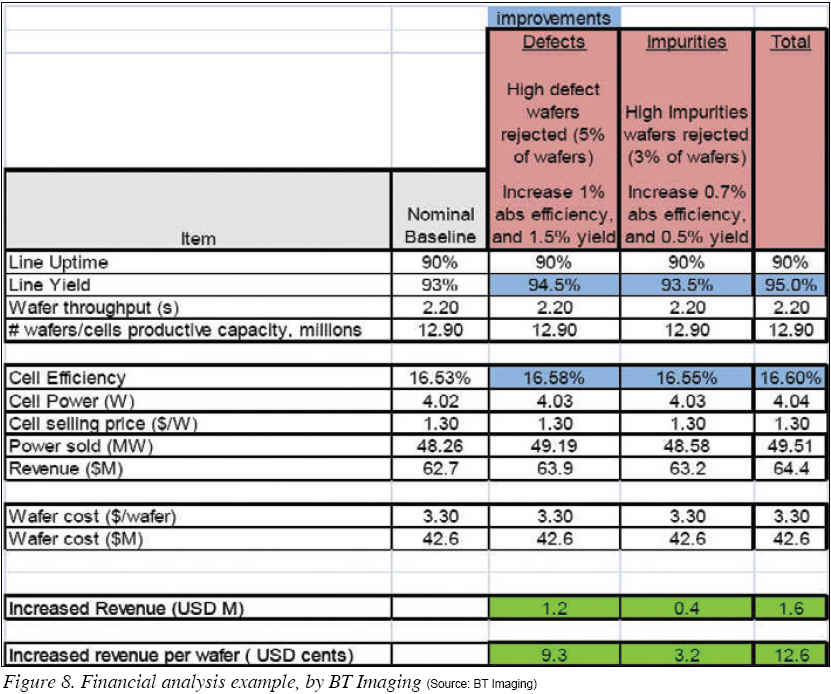
Financial Analysis
Based on the applications scenarios discussed earlier, a simple financial model can be used to estimate the financial benefit for a 40MW cell factory as shown in Figure 8.
-Cell factory revenue can be increased by not processing poor quality wafers;
-High-efficiency cell factory revenue can be increased by processing the best quality wafers;
-Wafer factory revenue can be increased by selling wafers with differential prices;
Summary
The following has been demonstrated:
-Defect density metrics can be determined on as cut wafers.
-These defect density metrics correlate with final cell electrical performance.
-The defect density metrics can be measured at production speeds with the iLS-W1.
High performing wafers can increase the revenue of a cell line without the need of any other changes.
Sophisticated cell manufacturers could use the electrical wafer quality data to gain a competitive advantage by employing special processing methods.
Given the demonstrated correlation between the BT Imaging electrical wafer quality metrics and cell performance, it is likely that cell manufacturers will require wafer manufacturers to qualify electrical wafer quality of wafers as a part of their final wafer inspection and sorting practice. Since cells are sold based on electrical output, it is likely that wafers will have differential pricing based on the electrical wafer quality specification.
W. McMillan, T. Trupke and J. Weber are working for BT Imaging Pty, Ltd (www.btimaging. com), M. Wagner and U. Mareck are for SolarWorld, Y.C. Chou is for Del Solar, J. Wong is for REC.
REFERENCES
1) Trupke, T., R.A. Bardos, and J. Nyhus, Photoluminescence characterization of silicon wafers and solar cells. 18th workshop on Crystalline Silicon Solar cells & Modules, 2008.
2) Cuevas, A. and D. Macdonald, Measuring and interpreting the lifetime of silicon wafers. Solar Energy, 2004. 76(1-3): p.255-262.
3) Sinton, R.A., et al., On the problem of determining the bulk lifetime of unpassivated silicon wafers. 14th workshop on Crystalline Silicon Solar cells and Modules, 2004.
4) Bothe, K., et al., Determination of th e bulk lifetime of bare multicrystalline silicon wafers. Progress in Photovoltaics: Research and Applications, 2010. 18: p. 204-208.
5) Haunschild, J., et al., Quality control of as-cut multicrystalline silicon wafers using photoluminescene imaging for solar cell production. Solar Energy Materials and Solar cells, accepted for publication.
6) Trupke, T., et al., Photoluminescence imaging of silicon wafers. Applied Physics Letters, 2006. 89: p. 044107.
7) Trupke, T., et al., Fast photoluminescence imaging of silicon wafers. WCPEC-4, Waikoloa, USA, 2006.
8) Haunschild, J., et al., Comparing luminescence imaging with illuminated lock-in thermography and carrier density imaging for inline inspection of silicon solar cells 24th European Photovoltaic Solar Energy Conference, Hamburg, September 2009, 2009.
9) Giesecke, J., et al., Spatially resolved characterization of silicon as-cut wafers with photoluminescence imaging. Progress in Photovoltaics: Research and Applications, 2009. 17(4): p.217-225
For more information, please send your e-mails to pved@infothe.com.
ⓒ2010 www.interpv.net All rights reserved. |


.jpg)