By Bjorn Hoffmann, Minna Toivola
.jpg)
 The ROD-SOL project, scheduled for three years, covered all parts of a typical solar cell development chain. Beginning at simulations of different nanowire solar cell concepts, a route towards substrate preparation, characterization and solar cell fabrication was set. Finally, the resulting prototype solar cells were analyzed and benchmarked by several project partners. Furthermore, the costs of a large-scale production of SiNW SCs were calculated and compared to common thin-film turnkey production lines. The ROD-SOL project, scheduled for three years, covered all parts of a typical solar cell development chain. Beginning at simulations of different nanowire solar cell concepts, a route towards substrate preparation, characterization and solar cell fabrication was set. Finally, the resulting prototype solar cells were analyzed and benchmarked by several project partners. Furthermore, the costs of a large-scale production of SiNW SCs were calculated and compared to common thin-film turnkey production lines.
A SiNW-layer offers improved optical properties compared to bulk or thin-film silicon. Due to an absorption cross section larger than a SiNW cross section if it is of the order of magnitude of an optical wavelength incident light will be absorped once it is scattered within a SiNW layer. Thus, the nanostructures act as optimal antireflective coating resulting in absorption of light in the visible range of over 90% though the SiNW-layer thickness did in no case exceed a few Ѕьm. Nevertheless, the SiNWs constitute also the active photovoltaic components of the cell which may pursuit various cell concepts. The most successful concept proved to be a Semiconductor-Insulator-Semiconductor (SIS) concept, where a 2 nm thin insulating layer acts as a tunneling barrier for minority charge carriers. This is, where Atomic Layer Deposition (ALD) techniques enter the scene. In the following section we will go into the details.
Preparation of the SiNW Solar Cells
The wires are formed in a wet-chemical etching process without any need of vacuum equipment. In the first step silver nanoparticles are randomly deposited on a wafer surface or a thin silicon layer on glass in a mixture of silver nitrate (AgNO3) and hydrofluoric acid (HF). In the second step these silver nanoparticles act as catalysts for silicon oxidation in a mixture of hydrogen peroxide (H2O2) and HF. The silicon dioxide (SiO2) formed in this catalytic reaction under the silver nanoparticle (AgNP) is etched away by the HF resulting in a movement of the AgNP into the silicon. In this way, a carpet of nanowires with defined length is formed. In the last step, the AgNPs are removed in concentrated nitric acid (HNO3). An electron microscopy image in Figure 1 shows the nanostructure of such a nanowire carpet.
.jpg)
From several tested solar cell concepts, a Semiconductor-Insulator-Semiconductor (SIS) architecture delivered the highest efficiencies of nearly 10%. Therefore, Atomic Layer Deposition (ALD) was utilized as it is the only technique that is able to form an extremely homogeneous ultrathin layer on such complex structures as our SiNWs due to its self-limiting monolayer deposition. The SIS fabrication process takes place in an ALD reactor where at first a 1.2nm thin tunneling barrier of Aluminum Oxide (Al2O3) and subsequently 400 nm of aluminum doped zinc oxide (AZO) as transparent front contact are deposited on the wires (see Figure 2). In order to get a defined tunneling barrier without pinholes, the deposition process uses a plasma assisted ALD method where reactive oxygen is used as oxidizing agent instead of water vapor.
After screen printing of a gold front contact grid, the solar cell is complete and ready for evaluation.
ALD and Its Possibilities in PV
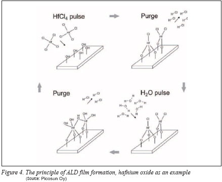
.jpg) Atomic layer deposition is a surface controlled, self-limiting chemical vapor processing method for manufacturing pinhole- and defect-free nanometer scale thin films of ultra-high uniformity, conformity, chemical and structural purity and exact thickness control. ALD process takes place in a vacuum chamber (typically 1-10 mbar) at elevated temperature (typically 200-400oC though with plasma-enhanced ALD processes working at even close to room temperature are possible), where gaseous precursor chemicals are introduced to the substrate surface in separate, alternating pulses between of which the chamber is flushed with inert gas such as nitrogen. The pulse-purge cycle is repeated till the desired film thickness is achieved (see Figure 4). Atomic layer deposition is a surface controlled, self-limiting chemical vapor processing method for manufacturing pinhole- and defect-free nanometer scale thin films of ultra-high uniformity, conformity, chemical and structural purity and exact thickness control. ALD process takes place in a vacuum chamber (typically 1-10 mbar) at elevated temperature (typically 200-400oC though with plasma-enhanced ALD processes working at even close to room temperature are possible), where gaseous precursor chemicals are introduced to the substrate surface in separate, alternating pulses between of which the chamber is flushed with inert gas such as nitrogen. The pulse-purge cycle is repeated till the desired film thickness is achieved (see Figure 4).
This separate pulse-purge procedure ensures the precursors wonЁЏt react until on the surface (unlike with other chemical vapor deposition techniques), so the ALD film grows along and ЁЎupЁЏ from the surface and the precursor molecules reach even the smallest nanoscale details of the surface. This enables coating both high aspect ratio nanostructures such as through-silicon-vias, microchannels, nanopores, rods and wires as well as planar or 3D substrates. ALD is easy to upscale simply by increasing the reactor sizeІЁalso roll-to-roll and in-line ALD systems which can be directly integrated to existing solar cell manufacturing lines have been developed.
The list of materials that can be deposited with ALD ranges from dielectrics to semiconductors, binary and ternary materials, metallic materials and even pure (also noble) metals and organic compounds. Due to the sequential, sub-nanometer scale controlled film growth and the self-controlling, self-limiting nature of the reaction chemistry between the precursor gases, atomic level organized and functionalized structures such as Nano laminates, graded or mixed layers and doped semiconductor films can be manufactured.
ALD is already widely in use in semiconductor, IC, MEMS, optics and sensor industries, but it is rapidly gaining foothold also in clean, sustainable and renewable energy technologies. In the PV industry, in addition to the enabling role ALD has in the novel SiNW solar cells developed in the project ROD-SOL, the method has huge potential in efficiency improvement and in replacing expensive and possibly toxic materials of also the ЁЎolderЁЏ generations of solar cells.
Al2O3 is one of the most well-known and widely used ALD materials and its deposition process is fast and simple. Al2O3 finds also several performance-improving applications in the field of PV. For crystalline silicon (c-Si) solar cells, passivation of the surface defects, ЁЎdanglingЁЏ H-bonds and other recombination promoting effects on the cell surface is a standard procedure in efficiency improvement. Typically, passivation has been achieved with thermally grown SiO2 or PECVD (plasma enhanced chemical vapor deposition) Si3N4 layers on the front side of the cell. However, ultra-thin ALD Al2O3 layers have also been successfully employed in this purpose. ALD Al2O3 passivation can be applied on both the front and back surface of the Si wafer, leading to 1-2 % absolute efficiency improvement, With just one side passivation, an impressive power conversion efficiency of 23.2 % has also been measured. This recombination velocity reducing property of ultra-thin Al2O3 passivation layers can be attributed to two mechanisms: chemical passivation, which arises from the reduction of the density of electronic surface states, and field-effect passivation, which originates from an internal electric field near the surface, i.e. reduction of the local electron or hole concentration.
Al2O3 is a superior passivation material compared to many others and ALD Al2O3 offers several benefits over the more conventional passivation methods. First of all, thermal oxidation of silicon requires high temperatures and thus lots of energy; also, the thermal stress may be detrimental to the bulk Si. With ALD, it is possible to use much lower deposition temperatures. Film is also pinhole-free and uniform and coats conformally even the most complicated nanoscale structures of the surface. ALD is also gentler to the surface than e.g., sputtering and other ion bombardment-based coating methods.
ALD-grown thin films have a wide variety of applications also in newer solar cell technologies. TCO (Transparent Conductive Oxide) layers used as current collectors in 2nd- and 3rd- generation photovoltaic devices such as CIGS, dye and organic solar cells and SiNW solar cells of ROD-SOL can be deposited with ALDІЁfor example, indium doped tin oxide (ITO) can be replaced with AZO to avoid problems arising from the scarcity and price of indiumІЁ and ALD-coated non-toxic, Cd-free buffer layers have yielded CIGS cells of even better efficiency than those prepared with traditional materials.
SiNW Solar Cell Characterization and Results
To determine the power conversion efficiency of the nanowire solar cell, a solar simulator with AM1.5 irradiation was used. Figure 5 shows the measured J-V curve in dark and under illumination and the corresponding properties: A short circuit current density of 35 mA/cmЉї is a quite high value that is achieved by the high absorption of light. The open-circuit voltage of 453 mV is also a respectable value for this early stage of development but has to be improved in the near future by optimization of surface passivation and contacts, which will also increase the fill factor.
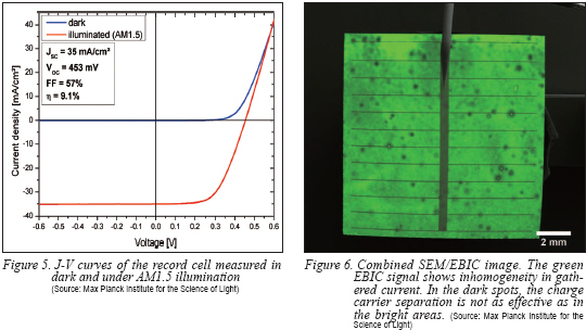
To check the cell for shunts and problems of homogeneity, Electron Beam Induced Current (EBIC) measurements were performed inside a Scanning Electron Microscope (SEM). With this method electron-hole pairs are generated by the incoming electron beam and the flowing current between the contacts is measured. In this way, a mapping of active regions, in which the charge carriers can be separated, is possible. Figure 6 shows a combined SEM/EBIC image where the EBIC signal is colored in green. The image shows that there are still problems with areas of lower charge carrier separation. On the other hand, there is no sign of large defects that totally annihilate the charge carrier collection.
Final Remarks
To conclude, the EU-funded project ROD-SOL has achieved very promising results. Nevertheless, a lot of possibilities for improvement were found in the cell analysis and, therefore, an efficiency of up to 15% is most likely achievable in the near future.
Bjorn Hoffmann received his diploma degree in solid state physics in 2008 from the University of Gottingen, Germany. Thereafter, he joined the group of PD Dr. Silke Christiansen at the Institute of Photonic Technology in Jena to perform his Ph.D. research about nanowire solar cells. This time he achieved the ROD-SOL record results presented in this article. Since 2012, he has worked at the Max Planck Institute for the Science of Light in Erlangen, Germany, as head of the electron microscopy lab.
Minna Toivola received her M.Sc. in physical chemistry in 1998 from the University of Helsinki, Finland. After working some years in Finnish high-tech companies, she joined the group of Prof. Peter Lund in the Dept. of Applied Physics at the Aalto University (former Helsinki University of Technology) to perform her research on dye solar cells. She received her D.Sc. (tech.) thesis in 2010. At Picosun Oy, she works as an EU project manager and also with the companyЁЏs marketing and communications. (www.picosun.com)
For more information, please send your e-mails to pved@infothe.com.
ЈЯ2011 www.interpv.net All rights reserved. |


.jpg)