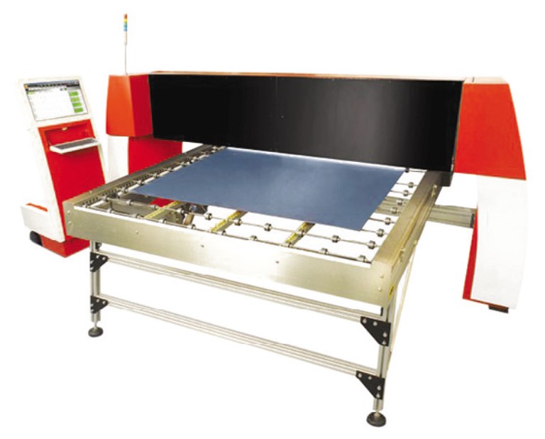
Figure 1. A Wide-Area-Metrology (WAM) Tool by BrightView Systems is designed for installation over existing lines and enables measurement of all production panels without interrupting line flow. Non-contact optical technology is utilized to extract multiple parameter maps on the fly. (Source: BrightView Systems)
By Ariel Ben-Porath and Benny Shoham
The proliferation of thin-film PV startups, mostly attributed to the 2008 raw silicon price hike, has resulted in several production technologies competing for dominance of the emerging thin-film PV market. For the largest thin-film segment―large glass panels for ground-based utility scale installations―more than 40 production lines will reach volume production and product certification by the middle of the year, and will be competing for project financing alongside c-Si and First Solar. Among these producers, about 75% will be utilizing turnkey lines by Oerlikon Solar, Applied Materials and Ulvac, a fact that may raise concerns regarding the capability of thin-film producers to differentiate their products and attract the attention of project integrators and financiers. Increasingly, the “bankability” of thin-film panels becomes a key factor driving this industry, by capturing the combined effect of several metrics, most notably the Leveliszed Cost of Energy (LCOE) and the risk associated with long-term system durability. Nevertheless, lessons of 2009 have taught the industry that substantial opportunities for innovation exist, allowing some thin-film manufacturers to rapidly achieve lower production costs, faster volume ramp-up and ensured product bankability. Most notably, Signet Solar Inc. has taken a leading role as an innovator of both technology and business models (AAA Ref: Signet Solar presentation at Thin Film Summit, San Francisco Dec 2009)
Process Optimization and Control Systems
An approach to achieving cost and bankability goals that is gaining momentum among thin-film producers is the incorporation of in-line process optimization solutions into turnkey production lines. This approach strives to marry the best of both worlds―the fast ramp-up and short time-to-market of turnkey solutions and the deep insight and understanding of process and device integration, that enables a producer to establish and execute a continuous improvement plan that drives product differentiation. In-line process optimization tools, such as process metrology and material characterization systems, can be retrofitted into existing lines or built into the design of new lines. In either case, such tools provide a thin-film manufacturer with a toolbox that is essential for further developing the process, reducing production costs and reaching the broad understanding of process and device integration that is required for achieving long-term product stability and durability.
The ability of a production line to produce highly identical modules, rather than a variety of modules that are later sorted into several product categories, is increasingly becoming a product differentiator in its own right. As production is mostly geared towards large ground-based systems, and the operators of such installations gain experience in the factors affecting the total energy harvesting of their arrays, the role of panel matching is emerging as a crucial factor. The variance between panel energy yields in an array is known to have a detrimental effect on the total energy yield, as chains and inverters effectively align themselves to their weakest members; however, the extent of the phenomenon has become apparent only with substantial statistical data coming out of installations that have been in operation for one or more years. It has become clear to project planners that panel matching holds the key to several percentage points of higher annual energy yield, and the subject is receiving attention. One of the approaches for counteracting the effects of non-uniformity―whether inherent or due to shading―has been the development and deployment of micro-inverters with each panel. Multiple solutions are on the market that take somewhat different approaches to achieve the same goal, however, they all include the addition of active electronic components onto each panel, which introduces a new set of reliability and durability concerns. If panels can be cost-effectively manufactured to higher matching requirements, total energy harvesting can be increased without requiring additional system components.
The potential for panel matching to improve energy harvesting reaches far beyond the stabilized panel efficiency, the common measure of a panel’s performance. With more accurate insight into the details of the production processes, including deposition, cleaning, scribing and encapsulation, higher matching can be achieved in other panel traits that play a role in the overall energy harvesting of an installation over its 25+ year lifetime. Changes in conversion efficiency, either due to temperature fluctuations or seasonal annealing, are most likely to be in higher correlation panels manufactured under a better controlled process. Research into these effects is in its infancy, yet theoretical predictions support this notion.
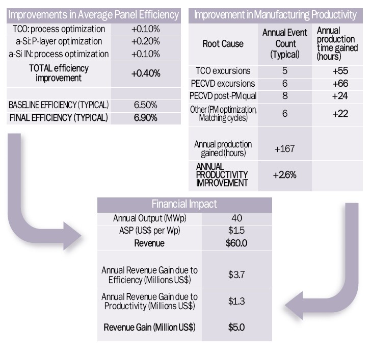
Table 1. Applying ROI modeling to the case of in-line wide-area-metrology in an amorphous Silicon production line. Improvements in module efficiency (Left) and improvements in line productivity (Right) are combined to reveal total financial implications (Bottom) (Source: BrightView Systems)
In-line Multilayer Mapping: Wide Area Metrology
In-line Wide Area Metrology (WAM) provides real-time mapping of absorber and contact layers, in the form of several panel maps that are generated on the fly (Figure 2). The WAM system by BrightView Systems (Figure 1) includes a non-contact optical metrology platform that combines multiple probes, a unique multispectral acquisition system and analysis software that enable measurements to be collected for 100% of the panels in production. Layer and material property maps are generated for such key metrics as layer and sub-layer thickness, layer surface topography and layer energy gap, and maintained in a global database. As a result, process control loops can be applied to specific tools, such as the PECVD deposition chambers, in order to optimize panel properties. One case study, shown in Figure 3 demonstrates how the average layer thickness that is computed from the two-dimensional thickness map is used as the control variable for achieving multiple chamber matching. Thin-film lines, in particular tandem and triple-junction lines, include up to several dozen chambers, and the capability to adjust individual chambers on-the-fly, without interrupting the flow of production, increases the total availability of the PECVD tools and provides a substantial benefit for deployment of in-line WAM.

Figure 2. Absorber deposition process health can be monitored via multiple parameter maps that are generated on the fly. (Left) A healthy thickness map for Si deposition, one of several parameters that are monitored simultaneously. (Right) A change to the spatial signature of the map due to a process problem that requires chamber maintenance. (Source: BrightView Systems)
ROI Model for In-line Wide Area Metrology
As the central component in several control loops, it is useful to develop the return-of-investment model for in-line Wide Area Metrology (WAM). While the details of the model would vary according to specific case strategies and line types, the general structure shown here applies in most cases. For the model, two main benefits of WAM deployment are:
● Improvements to average panel efficiency: Since increased panel efficiency with a given production process is almost directly convertible to lower manufacturing costs, such improvements that are achieved via process control loops are critical. In the model, individual layers (e.g., TCO coating, a-Si p-sub-layer deposition) are considered individually, as higher process capabilities can be achieved in each of these steps.
● Improvements to line productivity: These improvements are due to increased equipment availability, faster time to detection of process excursion and reduced maintenance and qualification times. Total panel yield―the number of good panels that are manufactured―is incorporated in this model into the line productivity arm.
Table 1 is an example of how the model can be applied to an a-Si line for estimating the additional revenue that is generated as a result of applying the in-line process control strategy. Additional benefits, due to improvements in panel matching for large-scale installations, are not included in this model and are currently under development.
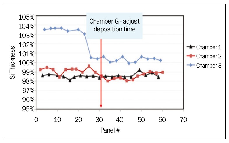
Figure 3. Real-time feedback enables adjustment of critical process parameters--deposition time, in this example. The average absorber thickness is extracted from in-line WAM maps for every panel, and three chambers are compared, and the rogue chamber is adjusted back into the process window. (Source: BrightView Systems)
As the thin-film PV industry emerges from its pilot stage to mass production, the competitive challenges and the reliance on turnkey lines will drive a surge of innovation that will fuel the quest for lower production costs, higher productivity and better panel matching. Turnkey lines will increasingly be perceived by both users and suppliers as starting points for process customization rather than fixed end-to-end solutions, and process enhancements will allow product differentiation and competitiveness. Process enhancement systems such as Wide Area Metrology tools will be a key component in driving this trend and provide tangible value for thin-film manufacturers.
Ariel Ben-Porath is VP of Marketing and Products at BrightView Systems
(http://www.brightview-sys.com/) and Benny Shoham is Co-founder and CEO of BrightView Systems.
For more information, please send your e-mails to pved@infothe.com.
ⓒ www.interpv.net All rights reserved
|


.jpg)