
By FIST IP Overview Team
[Editor’s Note]
The economic situation and, in particular, the upward trend in the price of fossil energies and political pressure on the markets induced in part by public opinion and in part by geopolitical aims to loosen the ties of energy dependence has meant that considerable budgets have been allocated over many years to the development of alternative energy sources. The production of photovoltaic electricity is one promising avenue among these various types of “clean energies”. Three main technological avenues exist for the photovoltaic energy production market: crystalline silicon cells (which represents in terms of patents nearly 3,300 families since 1985), thin-film cells (4,300 families) and organic cells (a little less than 1,900 families).
This article, which focuses on thin-film technology, represents the second in a series of three articles on the patent environment in the photovoltaic field. The first article published in the February 2010 issue of InterPV looked at patents and patent applications, filed between 1985 and mid 2007, that can be associated with crystalline silicon technology. The final article, available in the March 2010 issue, will examine organic and hybrid cell patent environment.
Protection Strategies
Evolution in Patent Filings
Despite a market that is still in its infancy, it may be observed that filings that concern photovoltaic technologies based on thin films are not a recent phenomenon. For instance, since 1985, between 150 and 200 filings have been made every year by the players involved in this sector. In recent years, a general increase in the annual number of filings up to around 250 patent applications a year may be noted, a potential sign of a new surge in interest for these technologies (since the data for 2007 is incomplete due to the 18 month delay in production, it has been extrapolated). Figure 1 illustrates the evolution over time of filings on photovoltaic thin film technologies.
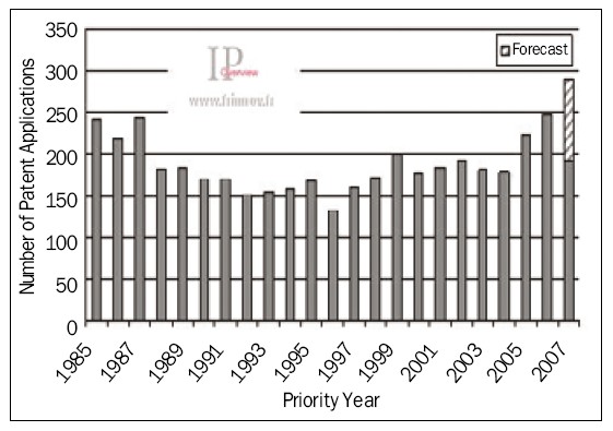
Figure 1. Evolution of thin-film cell patent filings (Source: FIST SA)
Priority Filings
An analysis of the location of the filings of priority patent applications results in the map shown in Figure 2. In keeping with the geographic origin of a large number of players in this sector as well as the practice of priority filing most frequently in the country of origin of the applicant, it is Japan that is the country where the largest number of priority filings is made (2,725 patent families). The overwhelming weight of priority filings in Japan since 1985 can also be explained by the fact that the Japanese patent office is traditionally tougher than other patent offices with regard to problems of the unity of invention. Japanese companies, therefore, file several patent applications with few claims in instances where an American or European company would only file one. The second is of an economic nature. In fact, the Japanese photovoltaic market has acted as a precursor and represents a high percentage of the global market. Moreover, Japanese firms are very well positioned in this field.
The major filing regions are then the United States (855 filings) and Germany (206 filings). The evolution over time of priority filings highlights a trend not shown up in the previous representation, namely that Japanese priority filings fell constantly over the studied period. Conversely, U.S., German and Chinese priority filings have risen sharply over recent years.
China, which still has a low volume of priority filings within its territory compared to all priority filings made since 1985, has now become an important motor for innovation in the sector. For instance, taking just 2007 as an example (for which the data is moreover incomplete), Chinese priority filings for that year were greater than the total number of all Chinese priority filings between 1985 and 2006. In fact, the Chinese government massively encourages the development of photovoltaic sourced energy, since it is faced with an ever increasing demand (4,200 TWh forecast in 2020), which necessitates a diversification of supply. Among Chinese applicants, it is interesting to note that numerous patent portfolios have been built up by academic institutions, such as that of the University of NANKAI (11 patent applications), the SHANGHAI Institute (8 filings), the University of SHANGHAI (6 patents) and the University of SICHUAN (5 patents).
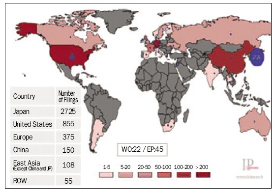
Figure 2. Map of priority filings concerning thin-film cells (Source: FIST SA)
Technological Maturity Factors
Analysis of the Evolution of Filings
Figure 3 illustrates past filing trends as well as the forecasts for coming years. For instance, a slight downturn in the general increase in the number of filings may be expected in 2009 linked to the economic situation, which could lead to massive cuts in patent protection budgets. In addition, the probable cut in R&D budgets in 2009, which may also extend into 2010, is likely to make its effects felt on the volume of patent application filings over the following years. Nevertheless, in the longer term, this sector should experience renewed growth due to the energy context (upward trend in the price of fossil energies) and political context (incentives in favor of renewable energies, Kyoto protocol). Growth is envisaged, with a volume of filings of around 300 patent applications a year within the next 4 years.
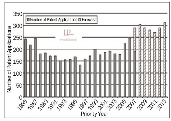
Figure 3. Forecast of the Number of Filings (Source: FIST SA)
Analysis of Industrial Filings over Time
Figure 4 illustrates the proportion of filings made either by industrial concerns or by academic institutions or instead jointly filed by an institution and an industrial player. “Other” filings mainly correspond to filings made in the names of inventors (in particular in the case of U.S. filings). As in most market sectors in which the immediate application of the patents is clearly identified, the majority of filings are made by industrial applicants, unlike more fundamental subjects where the proportion of academic institutions can attain 40% of filings. It is moreover interesting to note that joint filings between industrial concerns and institutional bodies are not very widely practiced in the photovoltaic field.
Nevertheless, the significant increase in the proportion of institutional filings compared to industrial filings since 2001 is worthy of note. In order to illustrate this point, the following graph shows the evolution over time of the filings made by major institutional bodies.
Such a representation clearly shows the increasing interest of Chinese and Korean institutions in this type of topic. Thus, over the last few years, the universities of NANKAI and SHANGHAI have filed in a sustained manner, as has KIST (Korea Institute of Science and Technology) and KIER (Korea Institute of Energy Research). The large number of filings made by the University of California should also be noted.
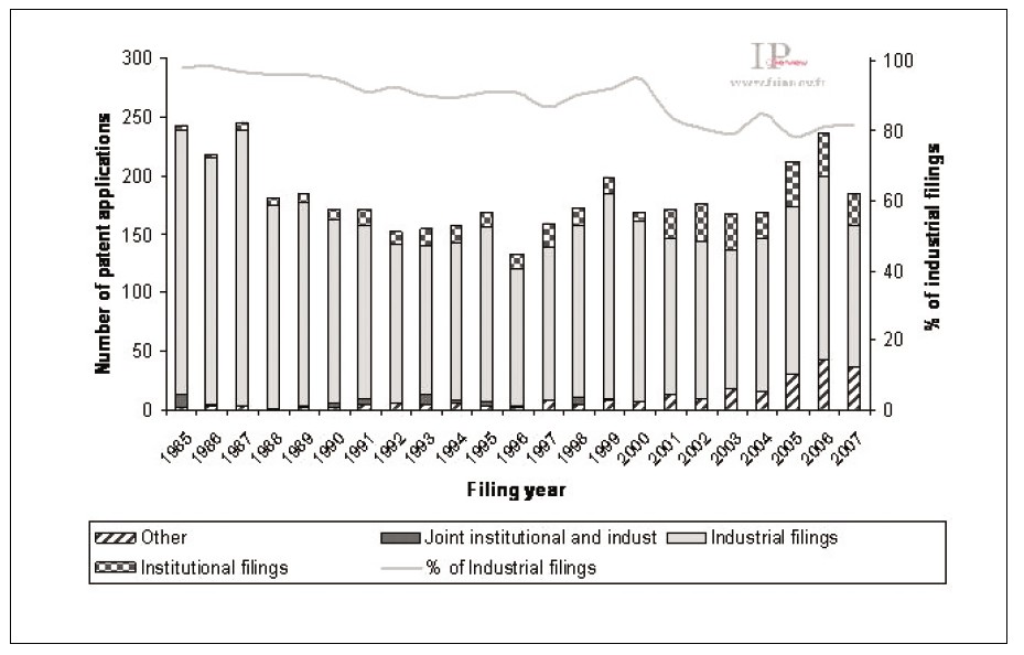
Figure 4. Evolution of the breakdown of industrial patents concerning thin-film cells (Source: FIST SA)
Topology of Portfolio Sizes
Figure 6 provides an insight into the composition of patent and patent application portfolios on photovoltaic thin-film cells. It appears that the majority of players (83%) have a portfolio of less than 5 patents and only 2% of patent portfolios contain more than 50 patents. A large number of players exist, including very small companies, universities and research centers, who file in the field without having a specific patent strategy.
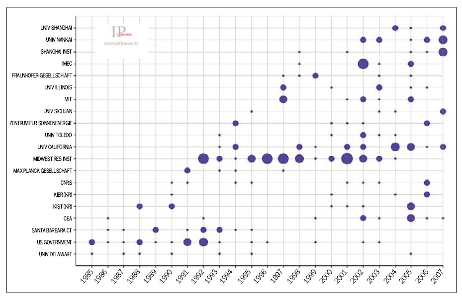
Figure 5. Evolution over time of filings made by academic institutions (Source: FIST SA)
Analysis of the Granting of Patents
It is interesting to analyze the proportion of patents granted as a function of the number of filings made. This analysis may be performed on U.S., Japanese and European filings and finally gives an insight into the real patent protection at the time of the study on which this article is based. It should be noted that the ratio of U.S. patents granted compared to U.S. patents filed has no sense here and needs to be extrapolated. In fact, before November 2000, U.S. patent applications were only published on the day of granting of the patent and applications that were not granted were never in fact published.
Thus, on the basis of the principle that the proportion of patents granted, filed before 2000, probably did not exceed 80% of the patents filed before this date, the U.S. data may be extrapolated as illustrated in Figure 7.
This figure shows that today, more patents have been granted in the United States than in Japan, which an analysis of the filings made previously could not predict.
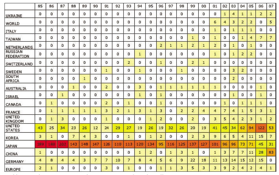
Table 1. Evolution in priority filings concerning thin-film cells (Source: FIST SA)
Evolution in the Number of Applicants
Figure 8 shows the evolution in the number of applicants who appear in the patent applications for the year in question (darker curve). Thus, this curve does not represent the total number of players active in the filing of patent applications, since a player may very well not have made any filings over the course of a year. The lighter curve, for its part, represents the annual number of applicants who appear for the first time in a patent application. An analysis of Figure 8 enables two principal trends to be identified:
● A first period from 1985 to 1997, during which the number of applicants oscillated between 40 and 70 every year, with the arrival of new applicants standing at about 20 newcomers a year.
● From 1997 onwards, a period of quite sustained growth in applicants up to 2006 may be observed, a sign of the increasing attractiveness of the sector, the number of new applicants also increasing overall.
Moreover, the data for 2006 provides a glimpse of a possible forthcoming surge in interest perhaps even more significant with nearly 55 newcomers in the sector for this year alone.
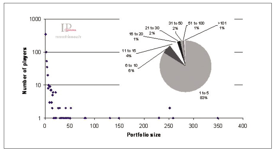
Figure 6. Portfolio size vs. number of players (Source: FIST SA)
Applicants
Major Applicants
As traditionally observed in the photovoltaic field, the major applicants are Japanese players (16 out of 20), 15 of which are industrial players. Two academic institutions are nevertheless included in this list of major applicants, the AIST (Japan’s leading public research centre) and the MIDWEST RESEARCH INSTITUTE. The MRI files in its own name patent applications stemming from the research work of the NREL (National Renewable Energy Laboratory) and also SolarTAC (Solar Technology Acceleration Center). MRI’s filings are not focused on a unique type of thin film cell, which is in keeping with the research topics announced in particular by NREL, namely: amorphous silicon (a-Si), copper indium diselenide (CuInSe2 or CIS) and related materials, cadmium telluride (CdTe), environment, safety, and health (ES&H), and module reliability.
The MATSUSHITA Group accounts for the largest number of filings, with in particular filings made by its different subsidiaries such as MATSUSHITA ELECTRIC, MATSUSHITA BATTERY and MATSUSHITA ECOLOGY. In fact, very early in the 1980s, MATSUSHITA positioned itself in thin film CdTe technologies (nearly half of the filings of MATSUSHITA concern this type of thin film) initially produced by screen printing and which generated thirty or so filings between 1985 and 1993. Subsequently, for the production of CdTe cells, MATSUSHITA turned towards close space sublimation techniques. In a more consequent manner, MATSUSHITA has also protected cells based on amorphous silicon (period between 1985 and 1990) before also focusing on the filing of patents concerning CIS cells (around 70 patent applications). Nevertheless, it should be noted that MATSUSHITA now only files a limited number of patent applications concerning photovoltaic thin film cells (around 3 to 4 applications a year since 2004).
FUJI ELECTRIC, whose patent and patent application portfolio exceeds 250 filings, began its research work in this sector in 1985 with filings initially focused on cells based on silicon, mainly deposited on glass substrates. Subsequently, several filings concerning CIS technology have been made by this company that does not seem to be focused on this type of technology. At present, in terms of commercialization, FUJI ELECTRIC has concentrated its efforts on the production of lightweight photovoltaic modules manufactured by laminating a film-type amorphous solar cell on a steel plate. Nevertheless, a reduction in the filing quantity by this company since 2005 (5 a year maximum) may be observed.
The SANYO Company also has a portfolio of around 250 families of patents on photovoltaic thin-film cells. Like numerous firms in the photovoltaic field, SANYO’s early efforts were concentrated on amorphous technologies. Thus SANYO, whose research began in 1975, started the mass production of amorphous cells for the general public in 1980. Correlatively, there were a very large number of patent filings on this subject over the period 1985-1995. Subsequently (as of 1990), the main topics cited in SANYO’s documents concern cells based on a layer of monocrystalline silicon coated with several thin films made of amorphous silicon (HIT technology─Heterojunction with Intrinsic Thin layer). The mass production of these cells started, for its part, in 1997. The current positioning of this company is thus a little different to that of other firms involved in the manufacture of thin film solar cells, since this type of cell favors high efficiency at low manufacturing costs.
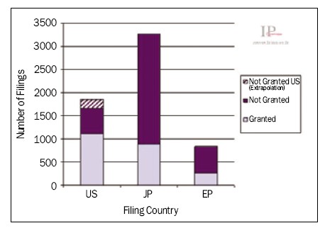
Figure 7. Overview of “Thin-film cell” granted patents (Source: FIST SA)
The patent applications of the SHARP Company (around 250 filings) reflect its strategic orientation towards multijunction cells. In particular, SHARP works on cells of this type based on the semiconductor InGaPAs (indium gallium phosphide arsenic) coupled to a concentrator. It has been possible to obtain a conversion efficiency of 40% for a cell of this type, with sides of 4.5 mm. The most recent patent applications are also turned towards multijunction cells comprising alternating amorphous silicon and microcrystalline silicon layers. The absence of filings made by SHARP concerning thin-film CIS/CIGS cells may also be noted.
Although the 4th player in the market, the absence of the FIRST SOLAR company among the major applicants is noteworthy. This company, specialized in the production and the commercialization of photovoltaic CdTe cells, only has in fact 8 patent applications on thin-film cells listed in the study. Nevertheless, an analysis of press releases shows that it collaborates closely with NREL (laboratory of the MIDWEST RESEARCH INSTITUTE, 18th applicant in the field and the 1st American applicant in the CdTe field).
Figure 10 illustrates the percentage share represented by the 10 leading applicants. Thus 42% of patents are held by these 10 major players. Such an observation is typical of a sector in which patent portfolios are still being built up but in which the major players are already in place. In fact, it is classical to observe, in sectors that are very technologically mature, much higher concentration ratios of patents, namely that 5 major players can share around 80% of patent filings in a given field.
Nevertheless, in this field it is important to keep in mind that the filing dynamic of the major players (in particular Japanese) is falling, which may falsify such an analysis.
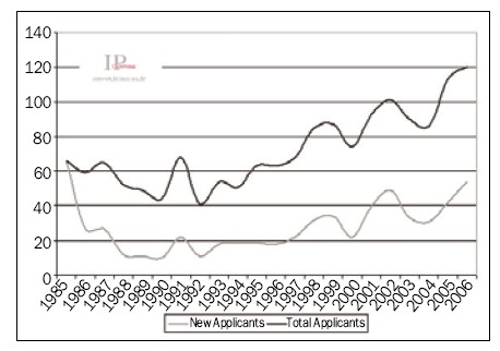
Figure 8. Evolution of the number of applicants (Source: FIST SA)
Emerging Application
Table 2 shows the companies or institutions that are starting to file, which we consider as “emerging applicants”. The emergence factor, which enables these applicants to be identified, corresponds to the growth in terms of patent filings over the period 2004, 2005, 2006 and 2007.
The NANOSOLAR Company was created in 2002 by two former students of STANFORD University. This company, which began to file patents in the photovoltaic field in 2002, is that which has shown the largest growth over the period 2004-2007. Its patent positioning ties in with its commercial announcements; in fact, out of the 21 patent applications, 15 explicitly concern CIGS cells. The characteristic of this company mainly resides in the deposition method that it uses, which is similar to newspaper printing techniques and has the advantage of taking place in a continuous manner on a flexible metal strip. At present, NANOSOLAR has two plants, one located in San Jose in California and the other near to Berlin in Germany, which represent an annual production capacity of 1GW.
APPLIED MATERIALS, with 15 filings between 2004 and 2007, is the second most dynamic company in the field in terms of recent filings. Unlike the companies previously described in this article, APPLIED MATERIALS does not, however, commercialize photovoltaic cells since the products of this company are exclusively aimed at equipment for photovoltaic thin film cell production lines. In particular, APPLIED MATERIALS has patents protecting multi-junction cells alternating thin films made of amorphous silicon with layers of microcrystalline silicon as well as the corresponding production equipment and processes. They have also protected through a patent a process and the related equipment enabling continuous deposition by electroplating on flexible substrates (US2008128013).
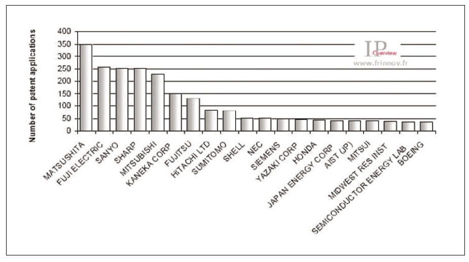
Figure 9. Major applicants in the field (Source: FIST SA)
The GE Company has pursued a dynamic filing policy in the photovoltaics sector from 2004 onwards, a period that was particularly marked by the takeover of ASTROPOWER, the photovoltaic equipment manufacturer, by the GE ENERGY branch. GE’s filing policy in the field began for its part in 2005 with 4 filings, followed by 7 in 2006 and at least 4 in 2007 (the delay in publication of the data prevents greater precision). The company has specially invested in “silicon nano-wire based” cells. Two key inventors of “GE’s solar platform” Tsakalakos LOUCAS and Korevaar BASTIAAN, are emerging inventors in the U.S.
KONARKA TECHNOLOGIES, a company based in Lowell, Massachusetts, was created in 2001. It is mainly focused on photovoltaic ink jet printing solutions on all types of substrate (plastic, fibres, etc.). This type of solution is dealt with in more detail in the article “Photovoltaics III - Organic Solar Cells” to be published in the April 2010 issue of InterPV. This company is very dynamic in terms of patent filings over the last few years (it has a portfolio of around 70 patent families). However, the ten or so patents that appear in this article dedicated to thin films mainly concern CIGS cells.
SOLYNDRA, based in Fremont, California, the U.S.A., was created in 2005 by Chris Gronet, who is still the company’s CEO. The company designs and manufactures photovoltaic systems composed of assembly panels and equipment for the commercial roofs market. It has in particular developed and protected, with ten or so patents, cylindrical modules and the technology of depositing suitable CIGS thin films. SOLYNDRA systems are designed to offer minimum installation costs for each system combined with maximum solar energy efficiency, mainly for roof applications. SOLYNDRA is a company in full economic and technological development. However, it should be noted that although Chris Gronet is the main inventor of SOLYNDRA patents, two key inventors left the company in 2008: Benyamin Buller for FIRST SOLAR (inventor in 4 SOLYNDRA patent applications filed in 2006, WO2008019066, WO2008060315, WO2007117442 and WO2008051275) and Ratson Morad for DAYSTAR TECHNOLOGIES (inventor of a SOLYNDRA patent filed in 2006, WO2008060315).
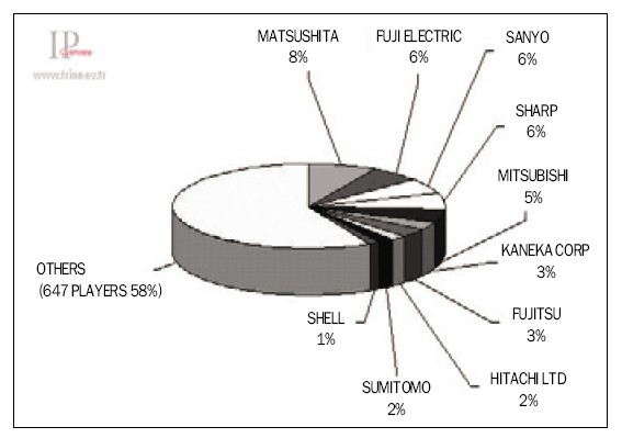
Figure 10. Breakdown of patent portfolios by applicant (Source: FIST SA)
Major Collaborations
There are different explanations to co-filings; they may, in fact, involve filings stemming from a collaboration between two separate companies, a collaboration between a company and an academic player, or instead the linkup may stem from a relation between a parent company with its subsidiary, which jointly file together.
For instance, the linkup that has generated the largest amount of co-filings is that between SIEMENS and ATLANTIC RICHFIELD COMPANY (ARCO). All of these co-filings took place between 1985 and 1988 before the takeover by SIEMENS of ARCO Solar in 1989 (the Californian subsidiary of ATLANTIC RICHFIELD OIL COMPANY). This takeover by SIEMENS allowed ARCO to become one of the main producers in the photovoltaic field at the time. The co-filings between these two companies mainly concerned CIS thin-film cells. The other most important collaboration in this sector is linked to the 8 co-filings of the TDK Company with the SEMICONDUCTOR ENERGY LAB, a Japanese private research laboratory.
Several co-filings between industrials correspond to jointly owned filings between a subsidiary and its parent company or instead a joint venture set up with a parent company, such as:
● SCHOTT with CARL ZEISS: both companies are 100% subsidiaries of the CARL ZEISS Foundation. The 9 co-filings between these two companies are mainly focused on aluminoborosilicate glasses.
● SIEMENS SHELL SOLAR with SHELL and SIEMENS: the majority of co-filings between SIEMENS, SHELL and their joint venture SIEMENS SHELL SOLAR relate to CIS thin-film cells and took place between 1993 and 1999.
Concerning the links between industrial players and institutions, SHARP’s filings with AIST are worth underlining, in particular, with regard to thin-film cells integrating microcrystalline silicon deposition.
The other noteworthy industrial/institutional collaboration concerns the linkup between EDF and CNRS, which has led to a joint research laboratory (CISEL) being set up on CIS thin-film cells.
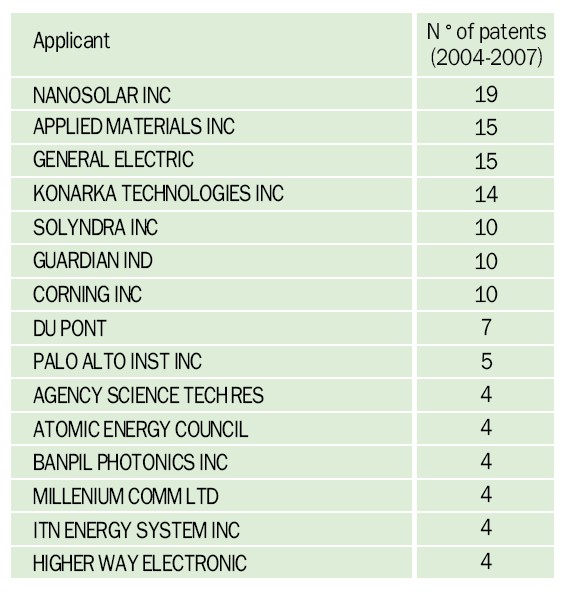
Table 2. Emerging applicants (Source: FIST SA)
Topology of Patents in Thin-film Cells
Segmentation of Patents by Technologies
The patent portfolios of photovoltaic technologies based on thin films is segmented in the following manner: the different types of cells as well as 3 categories that do not concern the type of cells, external connections, encapsulation and anti-reflective coatings, so as to identify the different positions taken by the players in the field.
Figure 11 shows that the type of thin film cells that have generated the most filings since 1985 are amorphous silicon cells, which account for nearly 1/4 of filings, followed by CdTe cells. Then come patents on solar cells based on micro- or nano-crystalline silicon thin films deposited on substrates, and CIS-CIGS and Ga-As multijunction solar cells, which each account for 10% of filings.
It is, nevertheless, important to observe these results over time so as not to have a biased view of the segmentation of filings by technology. In fact, although amorphous silicon thin-film cells have been researched for many years and have generated numerous filings, the production of patents concerning them has seen a fall over the last 20 years, the main drawback with these cells being their low efficiency. The same type of downward trend in terms of filings may also be observed in the case of CdTe cells, mainly for environmental concerns due to the fact that they contain cadmium.
Conversely, the number of patents concerning CIS-CIGS cells or even micro- or nano-crystalline silicon solar cells deposited on substrates has risen sharply over the last few years. Filings relating to multijunction cells are, for their part, increasing overall.
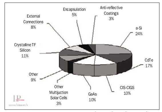
Figure 11. Segmentation of thin-film photovoltaic cell patent portfolios (Source: FIST SA)
Types of Cells Protected by the Major Players
Figure 13 enables the positions taken by different players that file patents on photovoltaic thin-film cells to be identified. Thus, some players have taken up exclusive or virtually exclusive positions on one type of thin-film cell, such as FUJITSU, NEC, JAPAN ENERGY CORP and NIPPON MINING for CdTe technologies. In the same way, YAZAKI CORP, HONDA, SHELL and NANOSOLAR are mainly focused on CIS/CIGS technologies. Other firms, such as FUJI ELECTRIC, KANEKA, MISTUBISHI and SHARP have patents that protect practically all types of thin-film cells.
Thin-film Cell Patents: The Complete Picture
The different market studies available for this sector predict an outlook of exponential growth of photovoltaic technology based on thin films. For example, the market assessment of NanoMarkets reports that this market should go from nearly 2.4 billion dollars in 2008 to more than 12 billion in 2013, i.e. growth of 50% a year. They base their analyses in particular on overall criteria such as the political willingness displayed by countries such as the U.S. and China to develop solar energy to diversify supply.
Among photovoltaic cells based on thin-film technologies, four major types may be distinguished:
● Cells based on the deposition of silicon, whether amorphous (a-Si), microcrystalline (μ-Si) or nanocrystalline (n-Si)
● Cells based on CdTe technology
● Cells based on CIS or CIGS technology
● And finally, other multijunctions, and principally cells based on Ga-As
The first three types, which are also the most widespread, have numerous shared advantages, which promises them a bright future in the context described previously. In fact, this type of technology enables deposition on large surfaces such as large glass plates, or even flexible substrates several hundreds of meters long. Their method of production is very advantageous compared to that of cells based on crystalline silicon, because continuous online production is possible, using very little raw material. The characteristics of this type of cell are very interesting, for example, with regard to their efficiency, which is in constant progress (up to 10% for a-Si, 16% for CdTe and 19% for CIS) or instead with regard to their very good resistance to exterior conditions. Finally, photovoltaic thin film cells are capable of meeting the needs of the most important market, i.e., the building sector, which requires a solution to turn roofs (industrial or private) into producers of electricity.
However, after nearly 30 years of research and development into these cells, they still only represent around 10% of the market and the revolution that is constantly being announced is constantly being put back...
The industrial environment of these technologies has not been very favorable, unlike crystalline silicon technology where silicon producers got on-board at an earlier stage. Glass manufacturers (such as SAINT GOBAIN, SCHOTT or CORNING), which would appear to be obvious suppliers of the substrates required for thin-film cells, only became involved in this technology at a relatively late stage. The first filings registered in this study date back to 1999 for SAINT GOBAIN and SCHOTT and only to 2005 for CORNING. The presence of Ulrich PEUCHERT and Peter BRIX, who file for SCHOTT GLAS-KARL ZEISS and who are among the most prolific European inventors, underlines the fact that glass makers are now fully-fledged participants in this technology and support it. Equipment manufacturers have generally held back before getting actively involved as well. APPLIED MATERIALS illustrates this point well. This company, which is specialized in deposition machines and high technology instrumentation, waited until 2006 to file its first patents. However, and in the image of glass manufacturers, its investment has been both considerable and rapid: 13 patents recorded by this article between 2006 and 2007, an inventor considered as an emerging inventor in the U.S. and numerous press releases announcing their arrival in the field.
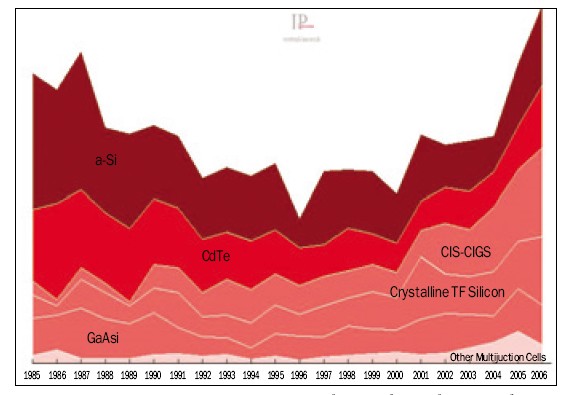
Figure 12. Segmentation of thin-film photovoltaic cell patent portfolios over time (Source: FIST SA)
Without a favorable industrial environment, thin-film cells cannot compete in terms of costs with their crystalline silicon rivals, the cost/power ratio being however the real key success factor. However, the new involvement of players linked to substrates and equipment in the specific field of thin films is going to change the situation in the medium term.
Although historically it is Japanese players that have dominated the intellectual property in the sector, the dynamism of patent filings is now being sustained by American players. In fact, although there were nearly 200 Japanese priority filings at the end of the 1980s (compared to a little more than twenty or so in the U.S.), nowadays there are around fifty or so in Japan compared to more than 120 in the U.S. To maintain a high level of innovation, the American and European players can count on the presence of numerous academic players (MIDWEST RESEARCH INSTITUTE, the UNIVERSITY OF CALIFORNIA or the HAHN MEITNER INSTITUTE). There are also a significant number of startups and very close collaborations between academic institutions and industry, made concrete through exploitation licenses. This innovation model is radically different to the Japanese model where industrial property is concentrated in the hands of 10 major players (MATSUSHITA, FUJI ELECTRIC, SANYO, SHARP, MITSUBISHI, KANEKA, FUJITSU, SUMITOMO, HITACHI and NEC).
An analysis of patents by technological thin-film segment makes it possible to illustrate several differences between them with regard not only to their technological maturity but also the industrial environment. In fact, even though the market is still only in its infancy, the race to build up strategic patent portfolios in these different technologies has already begun but the major different types of thin-film technology are at different technological maturity levels.
The most tried and tested technology and which covers half of the photovoltaic thin-film market (with 5.2% of the world photovoltaic market) is amorphous silicon technology. Even though this technology does not offer high efficiencies, it has the advantage of offering long lifetimes and, above all, a very accessible cost. It appears as the most mature technology among thin-film technologies and well positioned in the markets that it has conquered (markets linked to the supply of watches, calculators, emergency lighting, etc.) and only a technological revolution could push it into second position. Its major players, dominated by Japanese industrial concerns, are SHARP, FUJI ELECTRIC, MITSUBISHI and SANYO. In terms of industrial property, the drop in filings based on this technology is clearly observable, synonymous with players involved in the field backing out from research and development in the subject. Few major technological evolutions can thus be expected in this sector, unless perhaps two different areas of know-how are combined: crystalline silicon and amorphous silicon. This is in particular what SANYO is counting on. This company is the specialist in amorphous silicon cells and, since the 1990s, has developed photovoltaic cells based on its high performance HIT (Heterojunction with Intrinsic Thin layer) technology.
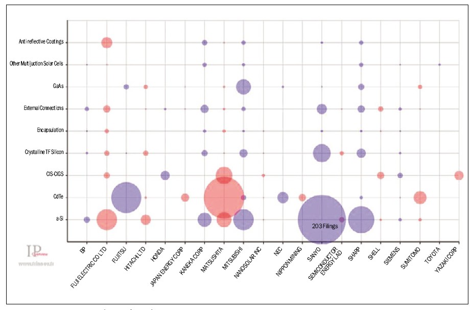
Figure 13. Topics of the major players (Source: FIST SA)
CdTe technology represents the second technology in terms of thin-film market share, with 4.7% of the world market. This technology benefits from the commercial success of the FIRST SOLAR Company, which has established itself as undisputed leader in this market segment. The principal patent portfolios belong to FIRST SOLAR, ANTEC SOLAR and especially MATSUSHITA and FUJITSU, which have locked out the technology through very early and massive filings. The large portfolios of the American research centers MIDWEST RESEARCH INSTITUTE and the UNIVERSITY OF CALIFORNIA are also worthy of note. At present industrial projects are multiplying, such as the creation of a plant by ABOUND SOLAR (representing an investment of 150 million dollars, the production startup of which was planned for early 2009). However, although this technology seems for the moment to be economically flourishing, the presence of cadmium risks acting as a brake to its expansion due to its toxicity. The number of filings in this technological segment has more or less stagnated over the last ten or so years.
The technological segment that shows the highest growth rate in terms of filings of priority patent applications is CIS technology. In 2006, the number of filings in this segment represented 25% of the total number of filings on thin films compared to 21% for a-Si, 17% for CdTe, 18.6% for thin films based on micro- or nano-crystalline silicon and 10.6% for Ga-As . The principal portfolios belong to SIEMENS, CIS SOLAR TECHNIK, BOEING, EDF/CNRS, KONARKA TECHNOLOGIES, NANOSOLAR, SOLYNDRA, HONDA and MATSUSHITA. It is the only segment that is not widely dominated by Japanese industrial players. European (IMEC, HAHN MEITNER INSTITUTE or the ZENTRUM FUR SONNENENERGIE) and American research institutes (the MIDWEST RESEARCH INSTITUTE or the UNIVERSITY OF CALIFORNIA) are also very active. This technology is still in the gestation stage and seems very promising for the future in terms of efficiency and price. A new European record for this type of cell has recently been claimed by the ZENTRUM FUR SONNENENERGIE UND WASSERSTOFFFORSCHUNG (ZSW): 19.6% efficiency for cells produced under pilot conditions using a multi-process line in an automated production plant. This result has been accredited by the Fraunhofer Institute for solar energy systems.
The other techniques based on thin films (the most developed being Ga-As heterojunctions) are more in search of efficiency performance than efficiency/cost ratio. The trend is towards niche markets such as aerospace or sports engine equipment (World Solar Challenge). Ga-As multijunction devices are the most efficient cells. For example, SPECTROLAB obtained a laboratory efficiency rate of 40.7% in 2006 and a team from the University of Delaware obtained a laboratory efficiency rate of 42.8% in 2007. The main problem with these types of technique based on gallium or germanium is their high cost, in particular, linked to the price of the raw materials used.
Thin-film technologies thus seem to be on the point of being capable of exploding in market terms. However, although the markets that they target are slightly different to crystalline silicon technologies and should enable them to co-exist with this technology, thin-film cells could nevertheless face stiff competition from organic and hybrid technologies (DSSC, Dye-Sensitized Solar Cell), whose potential is also promising but which are still in the technological maturation phase.
FIST IP Overview team (www.frinnov.fr) is expert in IP analysis and in the positioning of patent portfolio in many fields (memories, optical components, microscopy, HIV/AIDS, CDK inhibitors, Malaria, carbon nanotubes, green solvents, liquids effluents treatment, antenna, medical imaging, etc.). They developed the IP Overview product in 2008.
For more information, please send your e-mails to pved@infothe.com.
© www.interpv.net All rights reserved |


.jpg)