By Dr. Stefan Kontermann
The Black Silicon Laser Process
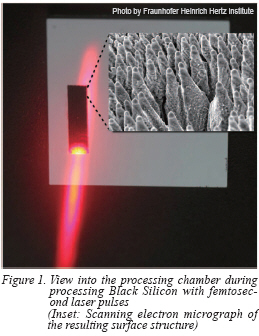 Bringing together a silicon wafer with some sulfuric ambient and blasting it with highly energetic femtosecond laser pulses will restructure the silicon surface on the nanoscale and simultaneously change the optoelectronic properties significantly. The surface structure enables perfect light trapping, while the incorporated sulfur turns the substrate Infrared (IR) active: The sulfur allows electrons to be excited across the band gap by absorption of two IR photons. The absorbed photons may have energies corresponding to wavelengths in the IR regime (λ > 1100 nm). The synthesized material is Black Silicon. It appears black, because light is perfectly trapped between the cone-like structures on its surface. Figure 1 shows the processing chamber during laser irradiation of the silicon substrate together with an inset revealing a Scanning Electron Micrograph (SEM) of the obtained surface structure. Bringing together a silicon wafer with some sulfuric ambient and blasting it with highly energetic femtosecond laser pulses will restructure the silicon surface on the nanoscale and simultaneously change the optoelectronic properties significantly. The surface structure enables perfect light trapping, while the incorporated sulfur turns the substrate Infrared (IR) active: The sulfur allows electrons to be excited across the band gap by absorption of two IR photons. The absorbed photons may have energies corresponding to wavelengths in the IR regime (λ > 1100 nm). The synthesized material is Black Silicon. It appears black, because light is perfectly trapped between the cone-like structures on its surface. Figure 1 shows the processing chamber during laser irradiation of the silicon substrate together with an inset revealing a Scanning Electron Micrograph (SEM) of the obtained surface structure.
Black Silicon Features
The outstanding advantage of femtosecond laser processed Black Silicon is, that the optical and electrical characteristics of the synthesized material can be adjusted over a wide range by varying the appropriate laser parameters. The surface structure is manipulable from nearly smooth over roughened to distinctively be spiked. This is shown in Figure 2.
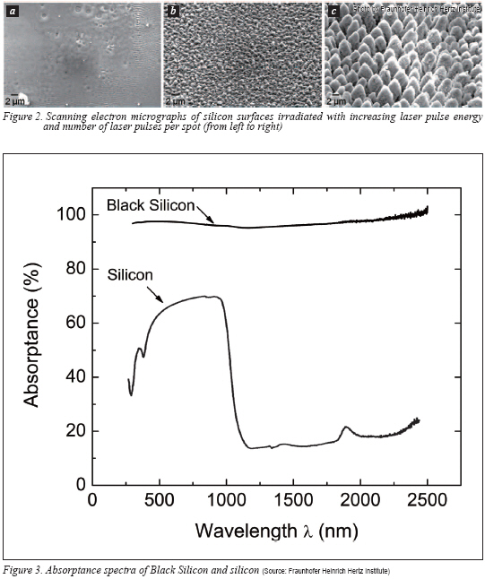
In Figure 2a, only one femtosecond laser pulse is applied. Apart from some ripples, the surface remains flat. Using five laser pulses yields a roughened structure as shown in Figure 2b. Increasing the laser fluence and maintaining the number of pulses in Figure 2c creates a structure comparable to a wet chemical random pyramid texture. With 500 pulses per spot, cone-like spikes form at the surface as displayed in the inset of Figure 1.
Figure 3 presents the optical absorption spectrum of Black Silicon in comparison to an unstructured silicon reference. It is revealed that the Black Silicon structure features a very low reflection. Black Silicon absorbs more than 95% of the incoming light for wavelengths between 250 nm < λ < 2500 nm. This wavelength range covers the visible and near infrared regime. The enhanced absorption in the visible wavelength range is caused by improved light trapping properties of the structured surface. Surprisingly Black Silicon perfectly absorbs light above a wavelength of λ = 1100 nm as well. This wavelength corresponds to an energy smaller than the band gap energy of silicon of 1.1 eV. The absorption of the black silicon sample at wavelengths above1100 nm remains above 95% in contrast to the reference sample, where the absorption at this wavelength drops below 10%. The IR absorption occurs, when laser processing takes place under sulfur or another chalcogen containing ambient.
The high IR absorption originates from the sulfur that introduces an energy level or, when available in sufficient concentration, forms an energy band within the band gap of silicon. Then photons with energies below the band gap energy can be absorbed. Less structured surfaces still feature the below band gap absorption, which is especially interesting, when surface recombination of charge carriers significantly matters in photovoltaic applications.
By incorporating sulfur into the silicon, not only IR absorption is realized, an n-type emitter is formed as well. The advantage is that the laser silicon interaction time scales are in the femtosecond regime, which drives the system of sulfur and silicon far out of equilibrium conditions and, therefore, allows for so called hyperdoping. This permits to incorporate more sulfur into the silicon than is allowed by its equilibrium solubility. Measuring the sulfur doping profile with Secondary Ion Mass Spectroscopy (SIMS) and calculating the appropriate sulfur concentration of a sample, laser structured under a sulfuric ambient gas, creates a shallow emitter containing potentially enough sulfur for obtaining on the one hand good lateral conductivity and on the other hand a low contact resistance.
Solar Cells on Black Silicon
Using Black Silicon as substrate allows to fabricate Black Silicon solar cells. For the Black Silicon laser process, the laser pulse shape was altered by optical laser pulse shaping equipment. With these shaped laser pulses, less crystal damage is achieved in the silicon during the laser silicon interaction. This facilitates minimizing surface recombination losses. The laser structuring itself simultaneously forms the front side texture and the emitter in one single process step, while it also modifies the raw silicon material enabling it to absorb the IR portion of the sun spectra.
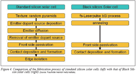
After laser structuring, evaporated front contacts and a screen printed rear contact are deposited. An edge isolation is not necessary, as the emitter is only formed on the front side. The process flow of the femtosecond laser processed Black Silicon solar cell is displayed in Figure 4 in comparison to the necessary process steps of a standard silicon solar cell. As the front side texturing and the emitter formation take place during the laser process, the total number of process steps is significantly reduced and can potentially cut production costs.
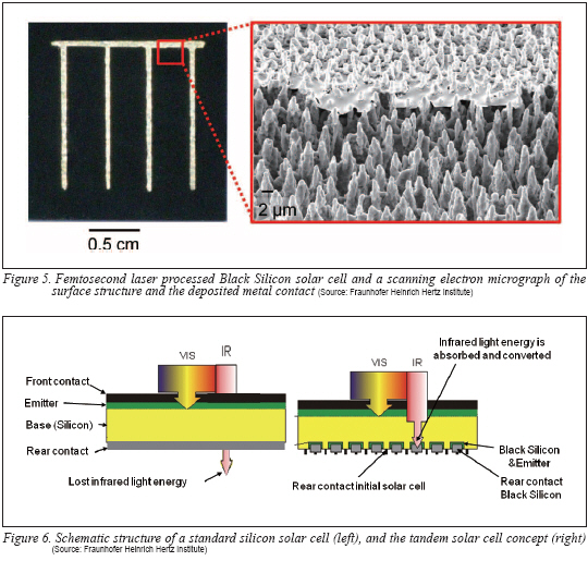
The finished solar cells display high short circuit current densities in the range of 38mA/cm2 < Jsc < 42mA/cm2 due to their increased absorption of IR light. We achieve an efficiency of 4.5% with no passivation layers applied. The previously reported record efficiency realized by Harvard University was 2.2% for a laser processed Black Silicon solar cell. Figure 5 presents the record Black Silicon solar cell together with a magnification of the silicon surface and the deposited metal contact.
Production Issues and Future developments
Currently, the laser processing speed for obtaining Black Silicon is 1 cm2/6 min. By using a laser with more output power, the beam can be expanded to more than 80 μm in diameter. Spot sizes of up to 1 cm2 at a fluence of 20 kJ/m2 are achievable with pulsed lasers, resulting in a structuring speed of 55 cm2/s meaning a structuring time of approximately 3s for a 125x125 mm2 wafer.
The Black Silicon laser process can be used for pure Black Silicon solar cells, but also for other applications, where a texture is necessary. One of our next steps is to optimize the laser process for a pure front side texture of silicon solar cells. As shown above in Figures 1 and 2, the structures induced by the femtosecond laser pulse process are highly variable. Therefore the laser process is well applicable to obtain a single side texture with adjustable surface features. This is especially interesting when single side textures are necessary in advanced solar cell concepts, e.g., the ‘Passivated Emitter and Rear Cell (PERC)’ concept. In a wet chemical texturing approach, both sides are generally textured in the bath, and protective layers need to be applied in additional processing steps. The most important advantage over wet chemical textures is, that the femtosecond laser induced surface structure is independent of the silicon crystal orientation. Therefore, this structuring method is perfectly suitable for texturing multicrystalline silicon wafers.
As the maximum achievable surface area magnification after laser structuring is approximately 700%, this laser structure can be used for improving the mechanical adhesive properties of specific solar cell coatings especially of plated layers for metallization purposes.
The overall efficiency of pure Black Silicon solar cells appears not yet to be competitive with the current performance of industrial solar cells. Therefore, we are developing a tandem solar cell, where Black Silicon for conversion of the normally lost IR light is partly implemented on the area of the rear side of an industrial standard silicon solar cell. The setup is shown in Figure 6. The basic idea of this tandem cell concept is to add the IR light conversion ability of the Black Silicon to the established silicon solar cell. For that reason, we integrate a second pn-junction formed by an area of Black Silicon on the back side of a standard industrial solar cell. The p-type substrate of the first cell acts as a base for both pn-junctions. The visual part of the solar spectrum is mainly absorbed in the first cell on the front side. The IR part of the spectrum passes the first pn-junction and can be harvested at the second Black Silicon pn-junction at the back side. As the energy of the IR portion of the sun spectrum represents 25% of the whole light energy contained in the sun spectrum, a pure Black Silicon solar cell and the tandem solar cell concept have the potential of increasing the efficiency of standard industrial silicon solar cells by 25%.
Dr. Stefan Kontermann heads the interdisciplinary research group ‘Nanomaterials for Energy Conversion’ that focuses on the synthesis of new functional materials by femtosecond laser technology at the Fraunhofer Heinrich Hertz Institute. Dr. Kontermann completed his Ph. D. in Physics at the University of Konstanz and the Fraunhofer Institute for Solar Energy Systems with additional research at the Lawrence Berkeley National Laboratory and the University of New South Wales, where he spear headed the optimization of the interface of metal silicon electrodes and developed new manufacturing processes for advanced silicon solar cell concepts.
For more information, please send your e-mails to pved@infothe.com.
ⓒ2011 www.interpv.net All rights reserved. |


.jpg)